V-I Characteristics, Circuit symbol, Example numerical problems - Zener diode | 12th Physics : UNIT 10a : Semiconductor Electronics
Chapter: 12th Physics : UNIT 10a : Semiconductor Electronics
Zener diode
Zener diode
Zener diode is a heavily doped
silicon diode used in reverse biased condition and is named after its inventor
C. Zener. It is specially designed to be operated in the breakdown region. The
doping level of the Silicon diode can be varied to have a wide range of
breakdown voltages from 2 V to over 1000 V.
As explained in the previous
section, Zener breakdown occurs due to the breaking of covalent bonds by the
strong electric field set up in the depletion region by the reverse voltage. It
produces an extremely large number of electrons and holes which constitute the
reverse saturation current. The current is limited by both external resistance
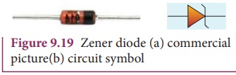
and power dissipation of the diode. A Zener diodes is shown in Figure 9.19(a)
and its circuit symbol of Zener diode is shown in Figure 9.19(b).
It looks like an ordinary p-n junction diode except the cathode lead approximating the shape of a ŌĆśzŌĆÖ letter. The arrow head points the direction of conventional current. In Figure 9.19(a), black ring indicates the cathode lead.
V-I Characteristics of Zener diode
The circuit to study the forward and
reverse characteristics of a Zener diode is shown in Figure 9.20(a) and Figure
9.20 (b). The V-I characteristics of a Zener diode is shown in Figure 9.20(c).
The forward characteristic of a Zener diode is similar to that of an ordinary
p-n junction diode. It starts conducting approximately around 0.7 V. However,
the reverse characteristics is highly significant in Zener diode. The increase
in reverse voltage ![]() normally
generates very small reverse current. While in Zener diode, when the reverse
voltage is increased to the breakdown voltage (VZ), the increase in
current is very sharp. The voltage remains almost constant throughout the
breakdown region. In Figure 9.20(c), IZ(max) represents the maximum reverse current. If the reverse current is
increased further, the diode will be damaged. The important parameters on the
reverse characteristics are
normally
generates very small reverse current. While in Zener diode, when the reverse
voltage is increased to the breakdown voltage (VZ), the increase in
current is very sharp. The voltage remains almost constant throughout the
breakdown region. In Figure 9.20(c), IZ(max) represents the maximum reverse current. If the reverse current is
increased further, the diode will be damaged. The important parameters on the
reverse characteristics are
VZ ŌåÆZener breakdown
voltage
IZ(min) ŌåÆ minimum current to sustain breakdown
IZ(max) ŌåÆ maximum current limited by maximum power dissipation.
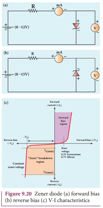
The Zener diode is operated in the reverse
bais having the voltage greater than VZ and current less than IZ(max).
The reverse characteristic is not exactly vertical which means that the diode
possesses some small resistance called Zener dynamic impedance. Zener
resistance is the inverse of the slope in the breakdown region. It means an
increase in the Zener current produces only a very small increase in the
reverse voltage. However this can be neglected. The voltage of an ideal Zener
diode does not change once it goes into breakdown. It means that VZ remains almost constant
even when IZ increases
considerably.
The maximum reverse bias that can be
applied before entering into the Zener region is called the Peak inverse
voltage. Commercially referred as PIV rating.
Applications
The zener diode can be used as
ŌĆó Voltage regulators
ŌĆó Calibrating voltages
ŌĆó Provide fixed reference voltage in
a network for biasing
ŌĆó Protection of any gadget against
damage from accidental application of excessive voltage.
Zener diode as a voltage regulator
A Zener diode working in the
breakdown region can serve as a voltage regulator. It maintains a constant output
voltage even when input voltage Vi
or load current IL varies.
The circuit used for the same is shown in Figure 9.21. Here in this circuit,
the input voltage Vi is regulated
at a constant voltage, Vz (Zener
voltage) at the output represented as V0
using a Zener diode. The output voltage is maintained constant as long as the
input voltage does not fall below Vz.
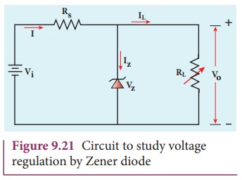
When the potential developed across
the diode is greater than VZ ,
the diode moves into the Zener breakdown region. It conducts and draws
relatively large current through the series resistance Rs. The total current I passing through Rs equals the sum of diode current
IZ and load current IL (I = IZ + IL ). It is to be noted that
the total current is always less than the maximum Zener diode current.
Under all conditions Vo =VZ . Thus, output voltage is regulated.
EXAMPLE: 9.3
Find the current through the Zener
diode when the load resistance is 1 K╬®. Use diode approximation.
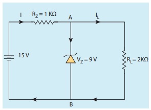
Solution
Voltage across AB is VZ =
9V
Voltage drop across R = 15 - 9 = 6V
Therefore current through the
resistor R,
I = 6 / 1├Ś103 =6 mA
Voltage across the load resistor = VAB = 9V
Current through load resistor
IL = VAB/RL
= 9 / 2├Ś103 = 4.5 mA
The current through the Zener diode,
IZ = I ŌłÆIL
=6 mAŌłÆ 4.5mA =1.5 mA
Related Topics