Semiconductor Electronics | Physics - Energy band diagram of solids | 12th Physics : UNIT 10a : Semiconductor Electronics
Chapter: 12th Physics : UNIT 10a : Semiconductor Electronics
Energy band diagram of solids
Energy band diagram of solids
In an isolated atom, the electronic
energy levels are widely separated and are far apart and the energy of the
electron is decided by the orbit in which it revolves around the nucleus.
However, in the case of a solid, the atoms are closely spaced and hence the
electrons in the outermost energy levels of nearby atoms influence each other.
This changes the nature of the electron motion in a solid from that of an
isolated atom to a large extent.
The valence electrons in an atom are
responsible for the bonding nature. Let us consider an atom with one electron
in the outermost orbit. It means that the number of valence electrons is one.
When two such atoms are brought close to each other, the valence orbitals are
split into two. Similarly the unoccupied orbitals of each atom will also split
into two. The electrons have the choice of choosing any one of the orbitals as
the energy of both the orbitals is the same. When the third atom of the same
element is brought to this system, the valence orbitals of all the three atoms
are split into three. The unoccupied orbitals also will split into three.
In reality, a solid is made up of
millions of atoms. When millions of atoms are brought close to each other, the
valence orbitals and the unoccupied orbitals are split according to the number
of atoms. In this case, the energy levels will be closely spaced and will be
difficult to differentiate the orbitals of one atom from the other and they
look like a band as shown in Figure 9.2. This
band of very large number of closely spaced energy levels in a very small
energy range is known as energy band.
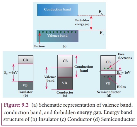
The energy band formed due to the valence orbitals is called
valence band and that formed due to the unoccupied orbitals to which electrons
can jump when energised is called the conduction band. The energy gap between
the valence band and the conduction band is called forbidden energy gap. Electrons cannot exist in the forbidden energy gap.
The representation of the valence
band and conduction band is shown in Figure 9.2(a). EV represents the maximum
energy of the valence band and EC represents minimum energy of the conduction
band. The forbidden energy gap, Eg = EC– Ev.
The kinetic energy of the electron increases from bottom to top (near the
nucleus to the farthest) and the potential energy decreases indicating that the
electrons in the orbitals closer to the nucleus are bound with large potential
energy. Hence, the electrons closer to nucleus require a lot of energy to be
excited. The electrons in the valence band are less bound to the nucleus and
can be easily excited.
The energy levels of the orbiting electrons are measured in electron volts, (eV).
Related Topics