Semiconductor Electronics | Physics - Multiple choice questions | 12th Physics : UNIT 10a : Semiconductor Electronics
Chapter: 12th Physics : UNIT 10a : Semiconductor Electronics
Multiple choice questions
BOOK BACK ONE WORDS:
1. The barrier
potential of a silicon diode is approximately,
a)
0.7 V
b)
0.3V
c)
2.0 V
d)
2.2 V
Answer: a)
2. Doping a
semiconductor results in
a)
The decrease in mobile charge carriers
b)
The change in chemical properties
c)
The change in the crystal structure
d)
The breaking of the covalent bond
Answer: c)
3. In an unbiased
p-n junction, the majority charge carriers (that is, holes) in the p-region
diffuse into n-region because of
a)
the potential difference across the p-n junction
b)
the higher hole concentration in p-region than that in n-region
c)
the attraction of free electrons of n-region
d)
the higher concentration of electrons in the n-region than that in the
p-region.
Answer: d)
4. If a positive
half-wave rectified voltage is fed to a load resistor, for which part of a
cycle there will be current flow through the load?
a)
0┬░-90┬░
b)
90┬░-180┬░
c)
0┬░-180┬░
d)
0┬░-360┬░
Answer: c)
5. The zener diode
is primarily used as
a)
Rectifier
b)
Amplifier
c)
Oscillator
d)
Voltage regulator
Answer: d)
6. The principle
based on which a solar cell operates is
a)
Diffusion
b)
Recombination
c)
Photovoltaic action
d)
Carrier flow
Answer: c)
7. The light
emitted in an LED is due to
a)
Recombination of charge carriers
b)
Reflection of light due to lens action
c)
Amplification of light falling at the junction
d)
Large current capacity
Answer: a)
8. The barrier
potential of a p-n junction depends on (i) type of semiconductor material (ii) amount
of doping (iii) temperature. Which one of the following is correct?
a)
(i) and (ii) only
b)
(ii) only
c)
(ii) and (iii) only
d)
(i) (ii) and (iii)
Answer: d)
9. To obtain
sustained oscillation in an oscillator,
a)
Feedback should be positive
b)
Feedback factor must be unity
c)
Phase shift must be 0 or 2ŽĆ
d)
All the above
Answer: d)
10. If the input to
the NOT gate is A = 1011, its output is
a) 0100
b)
1000
c)
1100
d)
0011
Answer: a)
Solution:
For
NOT Gate output Y = ߊ╣
Here
A = 1011 . Ōł┤ Y =0100
11. Which one of
the following represents forward bias diode?
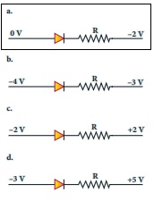
Answer: a)
12. The given electrical network is equivalent to

a)
AND gate
b)
OR gate
c)
NOR gate
d)
NOT gate
Answer: c)
Solution:
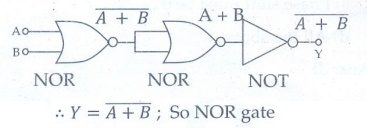
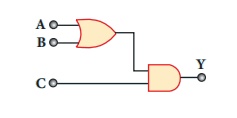
13. The output of
the following circuit is 1 when the input ABC is
a)
101
b)
100
c)
110
d)
010
Answer: a)
Solution:
Y
= (A+B)C
For
Y = 1; C must be 1
The
input ABC is 101
Y=
(1 + 0).l = 1
14. The variation of frequency
of carrier wave with respect to the amplitude of the modulating signal is
called _________
(a)
Amplitude modulation
(b)
Frequency modulation
(c)
Phase modulation
(d)
Pulse width modulation
Answer: b)
15. The frequency
range of 3 MHz to 30 MHz is used for
(a)
Ground wave propagation
(b)
Space wave propagation
(c)
Sky wave propagation
(d)
Satellite communication
Answer: c)
Multiple choice questions
1. The barrier potential of a silicon diode is approximately,
a. 0.7 V
b. 0.3V
c. 2.0 V
d. 2.2V
2. Doping a semiconductor results in
a. The decrease in mobile charge carriers
b. The change in chemical properties
c. The change in the crystal structure
d. The breaking of the covalent bond
3. A forward biased diode is treated as
a. An open switch with infinite resistance
b. A closed switch with a voltage drop of 0V
c. A closed switch in series with a battery voltage of 0.7V
d. A closed switch in series with a small resistance and a battery.
4. If a half ŌĆōwave rectified voltage is fed to a load resistor, which part of a cycle the load current will flow?
a. 0┬║ŌĆō90 ┬║
b. 90┬║ ŌĆō180┬║
c. 0┬║ ŌĆō180┬║
d. 0┬║ ŌĆō360┬║
5. The primary use of a zener diode is
a. Rectifier
b. Amplifier
c. Oscillator
d. Voltage regulator
6. The principle in which a solar cell operates
a. Diffusion
b. Recombination
c. Photovoltaic action
d. Carrier flow
7. The light emitted in an LED is due to
a. Recombination of charge carriers
b. Reflection of light due to lens action
c. Amplification of light falling at the junction
d. Large current capacity.
8. When a transistor is fully switched on, it is said to be
a. Shorted
b. Saturated
c. Cut-off
d. Open
9. The specific characteristic of a common emitter amplifier is
a. High input resistance
b. Low power gain
c. Signal phase reversal
d. Low current gain
10. To obtain sustained oscillation in an oscillator,
a. Feedback should be positive
b. Feedback factor must be unity
c. Phase shift must be 0 or 2ŽĆ
d. All the above
11. If the input to the NOT gate is A = 1011, its output is
a. 0100
b. 1000
c. 1100
d. 0011
12. The electrical series circuit in digital form is
a. AND
b. OR
c. NOR
d. NAND
13. Which one of the following represents forward bias diode?

Answer: Option a
Solution:

14. The given electrical network is equivalent to

a. AND gate
b. OR gate
c. NOR gate
d. NOT gate
15. The output of the following circuit is 1 when the input ABC is

a. 101
b. 100
c. 110
d. 010
Answers
1. a 2. c 3. d 4. c 5. d 6. c 7. a 8. b 9. c 10. d 11. a 12. a 13. a 14. c 15. a
Related Topics