Chapter: 12th Physics : UNIT 10a : Semiconductor Electronics
Types of Semiconductrors
TYPES OF SEMICONDUCTRORS
1. Intrinsic semiconductors
2. Extrinsic semiconductors: i. n-type semiconductor ii. p-type semiconductor
1. Intrinsic semiconductors
A semiconductor in its pure form without impurity is called an intrinsic semiconductor. Here, impurity means any other atom in the crystal lattice. The Silicon lattice is shown in Figure 9.3(a). Each Silicon atom has four electrons in the outermost orbit and is covalently bonded with the neighbouring atoms to form the lattice. The band diagram for this case is show in Figure 9.4(a).
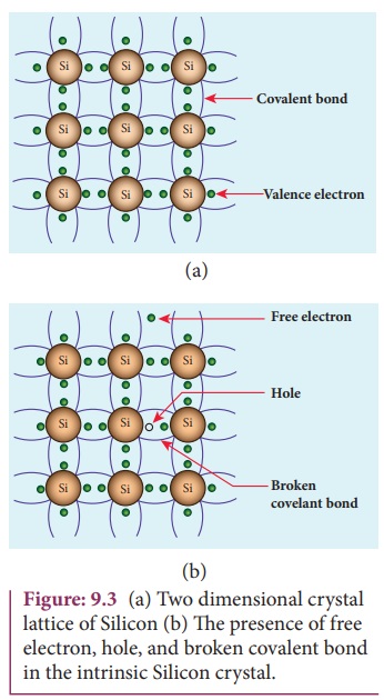
A small increase in temperature is sufficient enough to break some of the covalent bonds and release the electrons free from the lattice as shown in Figure 9.3(b). As a result, some states in the valence band become empty and the same number of states in the conduction band will be occupied as shown in Figure 9.4(b). The vacancies produced in the valence band are called holes. As the holes are deficiency of electrons, they are treated to possess positive charges. Hence, electrons and holes are the two charge carriers in semiconductors.
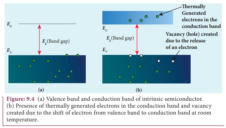
In intrinsic semiconductors, the number of electrons in the conduction band is equal to the number of holes in the valence band. The conduction is due to the electrons in the conduction band and holes in the valence band. These currents are represented as Ie and Ih respectively.
Definition of a hole: When an electron is excited, covalent bond is broken. Now octet rule will not be satisfied. Thus each excited electron leaves a vacancy to complete bonding. This ŌĆśdeficiencyŌĆÖ of electron is termed as a ŌĆśholeŌĆÖ
The total current (I ) is always the sum of the electron current (Ie ) and the hole current (Ih ) . I = Ie + Ih
An intrinsic semiconductor behaves like an insulator at 0 K. The increase in temperature increases the number of charge carriers (electrons and holes). The schematic diagram of the intrinsic semiconductor in band diagram is shown in Figure 9.4(b). The intrinsic carrier concentration is the number electron in the conduction band or the number of holes in the valence band in an intrinsic semiconductor.
2. Extrinsic semiconductors
The carrier concentration in an intrinsic semiconductor is not sufficient enough to develop efficient electronic devices. Another way of increasing the carrier concentration in an intrinsic semiconductor is by adding impurity atoms. The process of adding impurities to the intrinsic semiconductor is called doping. It increases the concentration of charge carriers (electrons and holes) in the semiconductor and in turn, its electrical conductivity. The impurity atoms are called dopants and its order is approximately 100 ppm (parts per million).
(i). n-type semiconductor
A n-type semiconductor is obtained by doping a pure Germanium (or Silicon) crystal with a dopant from group V pentavalent elements like Phosphorus, Arsenic, and Antimony as shown in Figure 9.5(a). The dopant has five valence electrons while the Germanium atom has four valence electrons. During the process of doping, a few of the Germanium atoms are replaced by the group V dopants. Four of the five valence electrons of the impurity atom are bound with the 4 valence electrons of the neighbouring replaced Germanium atom. The fifth valence electron of the impurity atom will be loosely attached with the nucleus as it has not formed the covalent bond.
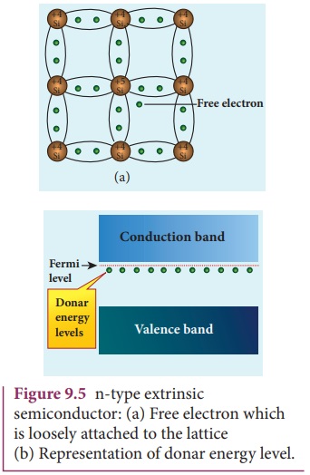
The energy level of the loosely attached fifth electron from the dopant is found just below the conduction band edge and is called the donor energy level as shown in Figure9.5(b). At room temperature, these electrons can easily move to the conduction band with the absorption of thermal energy. It is shown in the Figure 9.6. Besides, an external electric field also can set free the loosely bound electrons and lead to conduction.
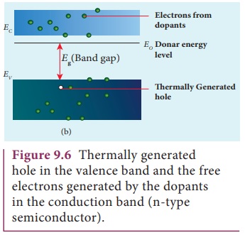
It is important to note that the energy required for an electron to jump from the valence band to the conduction band (Eg) in an intrinsic semiconductor is 0.7 eV for Ge and 1.1 eV for Si, while the energy required to set free a donor electron is only eV for Ge and 0.05 eV for Si.
The group V pentavalent impurity atoms donate electrons to the conduction band and are called donor impurities. Therefore, each impurity atom provides one extra electron to the conduction band in addition to the thermally generated electrons. These thermally generated electrons leave holes in valence band. Hence, the majority carriers of current in an n-type semiconductor are electrons and the minority carriers are holes. Such a semiconductor doped with a pentavalent impurity is called an n-type semiconductor.
(ii). p-type semiconductor
Here, a trivalent atom from group III elements such as Boron, Aluminium, Gallium and Indium is added to the Germanium or Silicon substrate. The dopant with three valence electrons are bound with the neighbouring Germanium atom as shown in Figure 9.7(a). As Germanium atom has four valence electrons, one electron position of the dopant in the Germanium crystal lattice will remain vacant. The missing electron position in the covalent bond is denoted as a hole.
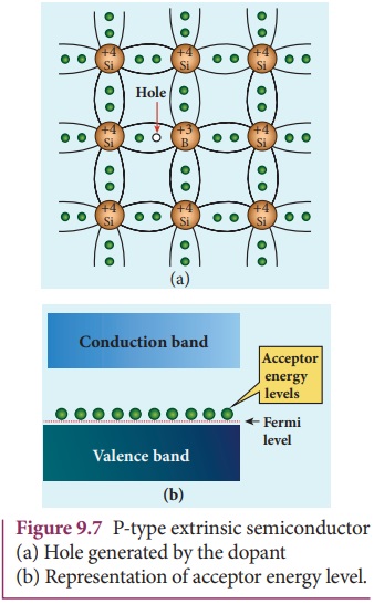
To make complete covalent bonding with all four neighbouring atoms, the dopant is in need of one more electron. These dopants can accept electrons from the neighbouring atoms. Therefore, this impurity is called an acceptor impurity. The energy level of the hole created by each impurity atom is just above the valence band and is called the acceptor energy level, as shown in Figure 9.7(b).
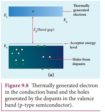
For each acceptor atom, there will be a hole in the valence band in addition to the thermally generated holes. In such an extrinsic semiconductor, holes are the majority carriers and thermally generated electrons are minority carriers as shown in Figure 9.8. The semiconductor thus formed is called a p-type semiconductor.
The n-type and p-type semiconductor are neutral as we are topping neutral atoms to the intrinsic semiconductors.
Related Topics