Biasing a diode, Circuit symbol, Schematic representation - P-N Junction diode | 12th Physics : UNIT 10a : Semiconductor Electronics
Chapter: 12th Physics : UNIT 10a : Semiconductor Electronics
P-N Junction diode
P-N Junction diode
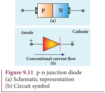
A p-n junction diode is formed when
a p-type semiconductor is fused with an-type semiconductor. It is a device with
single p-n junction as shown in Figure 9.11(a). The circuit symbol is shown in
Figure 9.11(b).
Biasing a diode
Biasing means providing external energy to charge carriers to
overcome the barrier potential and make them move in a particular direction. The charge carriers can either move towards the junction or away
from the junction. The external voltage
applied to the p-n junction is called
bias voltage. Depending on the polarity of the external source to the p-n
junction we have two types of biasing
1. Forward bias
2. Reverse bias
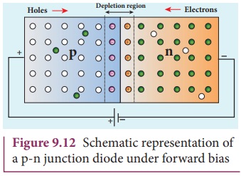
1. Forward Bias
If the positive terminal of the
external voltage source is connected to the p-side and the negative terminal to
the n-side, it is called forward biased as shown in Figure 9.12. The
application of a forward bias potential makes the electrons move into the
n-side and the holes into the p-side. This initiates the recombination with the
ions near the junction which in turn reduces the width of the depletion region
and hence the barrier potential.
The electron from the n-side is now
accelerated towards the p-side as it experiences a reduced barrier potential at
the junction. In addition, the accelerated electrons experience a strong
attraction by the positive potential applied to the p-side. This results in the
movement of electrons towards the p-side and in turn, holes towards the n-side.
When the applied voltage is increased, the width of the depletion region and
hence the barrier potential are further reduced. This results in a large number
of electrons passing through the junction resulting in an exponential rise in
current through the junction.
2. Reverse Bias
If the positive terminal of the
battery is connected to the n-side and the negative potential to the p-side,
the junction is said to be reverse biased as shown in Figure 9.13.
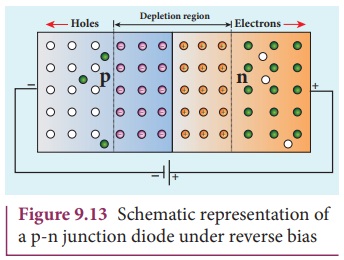
As the positive potential is
connected to the n-type material, the electrons in the n-type material are attracted
towards the positive terminal in turn, the holes in the p-type material move towards
the negative terminal (both away from the junction). It increases the immobile
ions at the junction. The net effect is the widening of the depletion region.
This leads to an increase in the barrier potential. Consequently, the majority
charge carriers from both sides experience a great barrier to cross the
junction. This reduces the diffusion current across the junction effectively.
Yet, a small current flows across
the junction due to the minority charge carriers in both regions. The reverse
bias for majority charge carriers serves as the forward bias for minority
charge carriers. The current that flows under a reverse bias is called the
reverse saturation current. It is
represented as Is .
The reverse saturation current is independent
of the applied voltage and it depends only on the thermally generated minority
charge carriers. Even a small voltage is sufficient enough to drive the
minority charge carriers across the junction.
The reverse saturation current of a
silicon diode doubles for every 10 °C rise in temperature.
Related Topics