Bipolar Junction Transistor [BJT] - Static Characteristics of Transistor in Common Emitter Mode | 12th Physics : UNIT 10a : Semiconductor Electronics
Chapter: 12th Physics : UNIT 10a : Semiconductor Electronics
Static Characteristics of Transistor in Common Emitter Mode
Static Characteristics of Transistor in Common
Emitter Mode
The know-how of certain parameters
like the input resistance, output resistance, and current gain of a transistor
are very important for the effective use of transistors in circuits. The
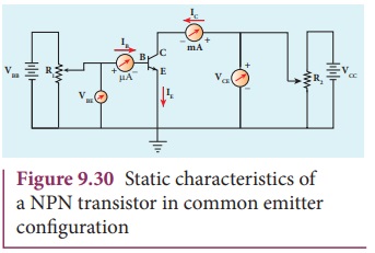
circuit to study the static characteristics of an NPN transistor in the common emitter
mode is given in Figure 9.30. The bias supply voltages VBB and VCC
bias the base-emitter junction and collector- emitter junction
respectively. The junction potential at the base-emitter is represented as VBE
and the collector-emitter as VCE. The rheostats R1and R2
are used to vary the base and collector currents respectively.
The static characteristics of the
BJT are
1. Input characteristics
2. Output characteristics
3. Transfer characteristics
1. Input Characteristics
Input Characteristics curves give
the relationship between the base current (IB
) and base to emitter voltage (VBE
) at constant collector to emitter voltage (VCE ) and are shown in Figure 9.31.
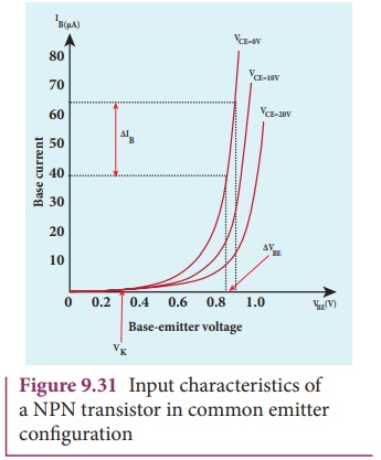
Initially, the collector to emitter voltage (VCE) is set to a particular voltage (above 0.7 V to reverse bias the junction). Then the base-emitter voltage (VBE) is increased in suitable steps and the corresponding base-current (IB) is recorded. A graph is plotted with VBE along the x-axis and IB along the y-axis. The procedure is repeated for different values of VCE.
The following observations are made from the graph.
ŌĆó The curve looks like the forward
characteristics of an ordinary p-n junction diode.
ŌĆó There exists a threshold voltage
or knee voltage (Vk ) below
which the base current is very small. The value is 0.7 V for Silicon and 0.3 V
for Germanium transistors. Beyond the knee voltage, the base current increases
with the increase in base-emitter voltage.
ŌĆó It is also noted
that the increase in the collector-emitter voltage decreases the base current.
This shifts the curve outward. This is because the increase in
collector-emitter voltage increases the width of the depletion region in turn,
reduces the effective base width and thereby the base current.
Input impedance
The ratio of the change in
base-emitter voltage (ŌłåVBE )
to the change in base current (ŌłåIB
) at a constant collector-emitter voltage (VCE) is called the input impedance (ri). The input impedance is not linear in the lower region
of the curve.
The input impedance is high for a transistor
in common emitter configuration.
2. Output Characteristics
The output characteristics give the
relationship between the variation in the collector current (Ōłå IC ) with respect to the
variation in collector-emitter voltage (ŌłåVCE
) at constant input current (IB
) as shown in Figure 9.32.
Initially, the base current (IB)
is set to a particular value. Then collector-emitter voltage (VCE)
is increased in suitable steps and the corresponding collector current (IC)
is recorded. A graph is plotted with the VCE along the x-axis and IC
along the y-axis. This procedure is repeated for different values of IB.
The four important regions in the output characteristics are:
(i) Saturation region
When VCE is increased above 0 V, the LC increases rapidly to a saturation value almost independent
of IB (Ohmic region, OA)
called knee voltage. Transistors are always operated above this knee voltage.
(ii) Cut-off region
A small collector current (IC) exists even after the
base current (IB ) is
reduced to zero. This current is due to the presence of minority carriers
across the collector-base junction and the surface leakage current (ICEO). This region is called
as the cut-off region, because the main collector current is cut-off.
(iii) Active region
In this region, the emitter-base
junction is forward biased and the collector-base junction is reverse biased.
The transistor in this region can be used for voltage, current and power
amplification.
(iv) Breakdown region
If the collector-emitter voltage (VCE ) is increased beyond the
rated value given by the manufacturer, the collector current (IC ) increases enormously leading
to the junction breakdown of the transistor. This avalanche breakdown can
damage the transistor.
Output impedance
The ratio of the change in the
collector-emitter voltage (ŌłåVCE
) to the corresponding change in the collector current (Ōłå IC ) at constant base current
(IB) is called output impedance
(rO).
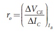
The output impedance for transistor
in common emitter configuration is very low.
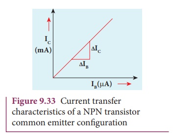
3. Current transfer characteristics
This gives the variation of
collector current (IC)
with changes in base current (IB
) at constant collector-emitter voltage (VCE ) as shown in Figure 9.33. It is seen that a small IC flows even when IB is zero. This current is
called the common emitter leakage current (ICEO
), which is due to the flow of minority charge carriers.
Forward current gain
The ratio of the change in collector
current (ŌłåIC ) to the
change in base current (ŌłåIB )
at constant collector-emitter voltage (VCE)
is called forward current gain (╬▓).
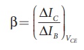
Its value is very high and it
generally ranges from 50 to 200. It depends on the construction of the transistor
and will be provided by the manufacturer. There are transistors with ╬▓ as high
as 1000 as well.
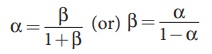
Relation
between ╬▒ and ╬▓
There is a relation between current gain in the common base
configuration ╬▒ and current gain in the common emitter configuration ╬▓ which is
given below.
╬▒ = ╬▓ / 1+
╬▓
(or) ╬▓ = ╬▒
/ 1 - ╬▒
EXAMPLE 9. 6
The output characteristics of a
transistor connected in common emitter mode is shown in the figure. Determine
the value of IC when VCE = 15 V. Also determine the value of IC when VCE is changed to
10 V.
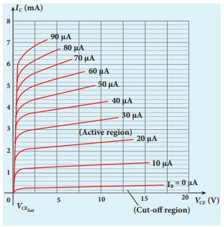
When VCE = 15 V, IC = 1.5 ╬╝A
When VCE is changed to 10 V,
IC
= 1.4 ╬╝A
The collector current is independent of the collector- emitter
voltage in the active region.
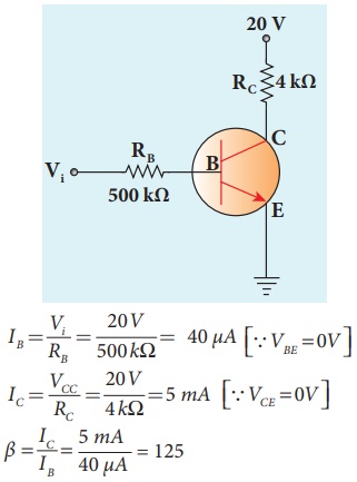
EXAMPLE 9.7
In the circuit shown in the figure,
the input voltage Vi is 20
V, VBE = 0 V and VCE = 0 V. What are the values of IB
, IC , ╬▓?
Related Topics