Chapter: 12th Physics : UNIT 10a : Semiconductor Electronics
Characteristics of a junction diode
Characteristics of a junction diode
Forward characteristics
It is the study of the variation in
current through the diode with respect to the applied voltage across the diode
when it is forward biased.
The p-n junction diode is forward
biased as shown in Figure 9.14(a). An external resistance (R) is used to limit the flow of current through the diode. The
voltage across the diode is varied by varying the biasing voltage across the dc
power supply. The forward bias voltage and the corresponding forward bias
current are noted. A graph is plotted by taking the forward bias voltage (V) along the x-axis and the current (I) through the diode along the y-axis.
This graph is called the forward V-I
characteristics of the p-n junction diode and is shown in Figure 9.14(b).
Three inferences can be brought out from the graph:
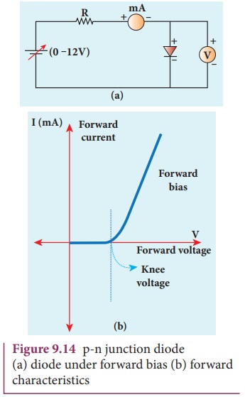
(i) At room temperature, a potential
difference equal to the barrier potential is required before a reasonable
forward current starts flowing across the diode. This voltage is known as threshold voltage or cut-in voltage or knee
voltage (Vth). It is approximately 0.3 V for Germanium and 0.7 V
for Silicon. The current flow is negligible when the applied voltage is less
than the threshold voltage. Beyond the threshold voltage, increase in current
is significant even for a small increase in voltage.
(ii) The graph clearly infers that
the current flow is not linear and is exponential. Hence it does not obey OhmŌĆÖs
law.
(iii) The forward resistance (rf) of the diode is the ratio
of the small change in voltage (ŌłåV ) to the small change in current (ŌłåI ), rf
= ŌłåV/ŌłåI.
(iv) Thus the diode behaves as a
conductor when it is forward biased.
However, if the applied voltage is
increased beyond a rated value, it will produce an extremely large current
which may destroy the junction due to overheating. This is called as the
breakdown of the diode and the voltage at which the diode breaks down is called
the breakdown voltage. Thus, it is safe to operate a diode well within the
threshold voltage and the breakdown voltage.
Reverse characteristics
The circuit to study the reverse
characteristics is shown in Figure 9.15(a). In the reverse bias, the p-region
of the diode is connected to the negative terminal and n-region to the positive
terminal of the dc power supply.
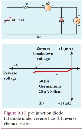
A graph is drawn between the reverse
bias voltage and the current across the junction, which is called the reverse
characteristics of a p-n junction diode. It is shown in Figure 9.15(b). Under
this bias, a very small current in ┬ĄA, flows
across the junction. This is due to the flow of the minority charge carriers
called the leakage current or
reverse saturation current. Besides, the current is almost independent of the
voltage. The reverse bias voltage can be increased only up to the rated value
otherwise the diode will enter into the breakdown region.
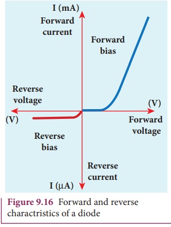
The forward and reverse
charactristics are given in one graph as shown
in Figure 9.16.
Ideal diode: It acts like a
conductor when it is forward biased. When it is reverse biased, it acts like an
insulator. The barrier potential is assumed to be zero and hence it behaves
like a resistor.
EXAMPLE 9. 1
An ideal diode and a 5 ╬® resistor are connected in series with a 15 V power supply
as shown in figure below. Calculate the current that flows through the diode.
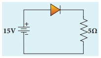
Solution
The diode is forward biased and it is
an ideal one. Hence, it acts like a closed switch with no barrier voltage.
Therefore, current that flows through the diode can be calculated using OhmŌĆÖs
law.
V = IR
I =V/R
= 15/5 = 3 A
EXAMPLE 9. 2
Consider an ideal junction diode.
Find the value of current flowing through AB is
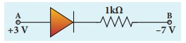
Solution
The barrier potential of the diode
is neglected as it is an ideal diode.
The value of current flowing through
AB can be obtained by using OhmŌĆÖs law
I = V/R = 3 - (-7) / 1├Ś 103 /103 = 10 =10-2
A = 10mA
Related Topics