Diodes | Semiconductor Electronics | Physics - P-N Junction formation | 12th Physics : UNIT 10a : Semiconductor Electronics
Chapter: 12th Physics : UNIT 10a : Semiconductor Electronics
P-N Junction formation
P-N Junction formation
Formation of depletion layer
A p-n junction is formed by joining n-type and p-type
semiconductor materials as shown in Figure 9.9(a). Since the n-region has a high electron
concentration and the p-region a high
hole concentration, electrons diffuse from the n-side to the p-side.
This causes diffusion current which
exists due to the concentration difference of electrons. The electrons
diffusing into the p-region may occupy holes in that region and make it
negative. The holes left behind by these electrons in the n-side are equivalent to the diffusion of holes from the p-side to the n-side. If the electrons and holes were not charged, this diffusion
process would continue until the concentration of electrons and holes on the
two sides were the same, as happens if two gasses come into contact with each
other.
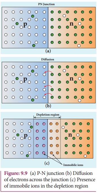
But, in a p-n junction, when the
electrons and holes move to the other side of the junction, they leave behind exposed
charges on dopant atom sites, which are fixed in the crystal lattice and are
unable to move. On the n-side,
positive ion cores are exposed and on the p- side, negative ion cores are exposed
as shown in Figure 9.9(b). An electric field E forms between the positive ion
cores in the n-type material and
negative ion cores in the p-type
material. The electric field sweeps free carriers out of this region and hence
it is called depletion region as it is depleted
of free carriers. A barrier potential Vb due to the electric field E
is formed at the junction as shown in Figure 9.9(c).
As this diffusion of charge carriers
from both sides continues, the negative ions form a layer of negative space
charge region along the p-side. Similarly, a positive space charge region is
formed by positive ions on the n-side. The positive space charge region
attracts electrons from p-side to n-side and the negative space charge region
attracts holes from n-side to p-side. This moment of carriers happen in this
region due to the formed electric field and it constitutes a current called
drift current. The diffusion current and drift current flow in the opposite
direction and at one instant they both become equal. Thus, a p-n junction is
formed.
Junction potential or barrier potential
The recombination of charge carriers
takes place only to a certain point beyond which the depletion layer acts like
a barrier to further diffusion of free charges across the junction.
This is due to the fact that the
immobile ions on both sides establish an electric potential difference across
the junction. Therefore, an electron trying to diffuse into the interior of the
depletion region encounters a negative wall of ions repelling it backwards. If
the free electron has enough energy, it can break through the wall and enter
into the p-region, where it can recombine with a hole and create another
negative ion.
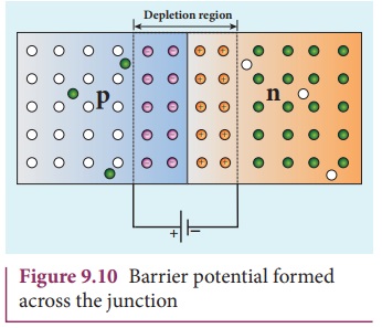
The strength of the electric
potential difference across the depletion region keeps increasing with the
crossing of each electron until equilibrium is reached; at this point, the
internal repulsion of the depletion layer stops further diffusion of free
electrons across the junction. This difference in potential across the
depletion layer is called the barrier
potential as shown in Figure 9.10. At 25ÂşC, this barrier potential
approximately equals 0.7 V for Silicon and 0.3 V for Germanium.
Related Topics