Bipolar Junction Transistor [BJT] - Transistor action in the common base mode | 12th Physics : UNIT 10a : Semiconductor Electronics
Chapter: 12th Physics : UNIT 10a : Semiconductor Electronics
Transistor action in the common base mode
Transistor action in the common base mode
The operation of an NPN transistor
in the common base mode is explained below. The current flow in a common base
NPN transistor in the forward active mode is shown in Figure 9.29.
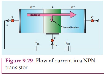
Basically, a BJT can be considered
as two p-n junction diodes connected back- to-back. In the forward active bias
of the transistor, the emitter-base junction is forward biased by a dc power
supply VEB and the collector-base junction is reverse biased by the bias
power supply VCB. The forward bias decreases the depletion region
across the emitter-base junction and the reverse bias increases the depletion
region across the collector-base junction. Hence, the barrier potential across
the emitter-base junction is decreased and the collector-base junction is
increased. The voltage across the emitter-base junction is represented as VEB
and the collector-base junction as VCB.
In an NPN transistor, the majority
charge carriers in the emitter are electrons. As it is heavily doped, it has a
large number of electrons. The forward bias across the emitter- base junction causes
the electrons in the emitter region to
flow towards the base region and constitutes the emitter current (IE) . The electrons after reaching
the base region recombine with the holes in the base region. Since the base
region is very narrow and lightly doped, all the electrons will not have
sufficient holes to recombine and hence most of the electrons reach the
collector region.
Eventually, the electrons that reach
the collector region will be attracted by the collector terminal as it has
positive potential and flows through the external circuit. This constitutes the
collector current (IC ) .
The holes that are lost due to recombination in the base region are replaced by
the positive potential of the bias voltage VEE and constitute the base
current (IB) . The magnitude of the base current will be in
micoamperes as against milliamperes for emitter and collector currents.
It is to be noted that if the
emitter current is zero, then the collector current is almost zero. It is
therefore imperative that a BJT is called a current controlled device. Applying
Kirchoff ŌĆÖs law, we can write the emitter current as the sum of the collector
current and the base current.
IE = IB + IC
![]() Since
the base current is very small, we can write, IE Ōēł IC
. There is another component of collector current due to the thermally
generated electrons called reverse saturation current,
denoted as (ICO ). This factor
is temperature sensitive. Therefore, care must be taken towards the stability
of the system at high temperatures.
Since
the base current is very small, we can write, IE Ōēł IC
. There is another component of collector current due to the thermally
generated electrons called reverse saturation current,
denoted as (ICO ). This factor
is temperature sensitive. Therefore, care must be taken towards the stability
of the system at high temperatures.
The ratio of the collector current
to the emitter current is called the forward current gain (╬▒dc ) of a transistor.
╬▒dc = IC / IE
The ╬▒ of a transistor is a measure
of the quality of a transistor. Higher the value of ╬▒ better is the transistor. It means that the collector
current is closer to the emitter current. The value of ╬▒ is less than unity and
ranges from 0.95 to 0.99. This indicates that the collector current is 95% to
99% of the emitter current.
1. The conventional flow of current
is based on the direction of the motion of holes
2. In NPN transistor, current enters
from the base into the emitter.
3. In a PNP transistor, current
enters from the emitter into the base.
4. The emitter-base junction has low
resistance and the collector-base junction has high resistance.
Working of a PNP transistor
The working of a PNP transistor is
similar to the NPN transistor except for the fact that the emitter current IE is due to holes and the
base current IB is due to
electrons. However, the current through the external circuit is due to the flow
of electrons.
EXAMPLE 9. 5
In a transistor connected in the
common base configuration, ╬▒=0.95 , IE
=1 mA . Calculate the values of IC and IB .
Solution
╬▒= IC/IE
IC =╬▒ IE =0.95├Ś1=0.95 mA
IE = IB + IC
Ōł┤ IB
= IC ŌłÆIE =1ŌłÆ0.95=0.05 mA
Related Topics