Semiconductor Electronics | Physics - Summary, Concept Map | 12th Physics : UNIT 10a : Semiconductor Electronics
Chapter: 12th Physics : UNIT 10a : Semiconductor Electronics
Summary, Concept Map
Semiconductor Electronics | Physics
SUMMARY
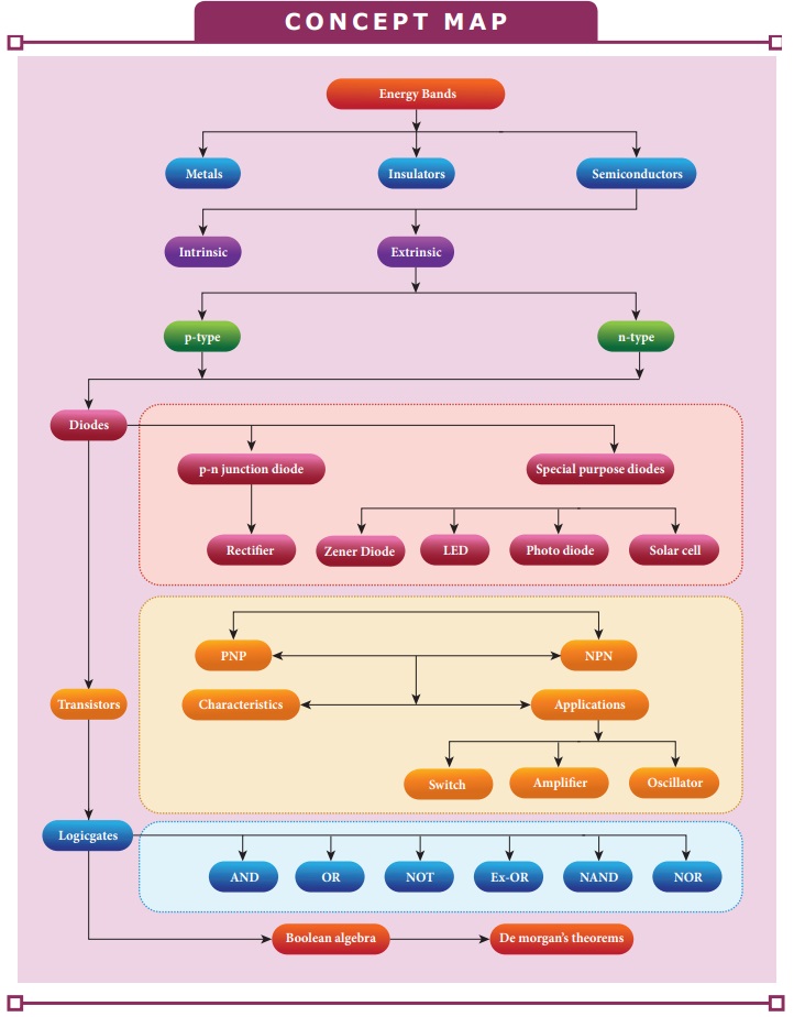
• Energy bands in solids are used to classify them
into metals, insulators, and semiconductors
• In a N-type semiconductor, electrons are the
majority charge carriers and holes are the minority carriers
• In P-type semiconductor, holes are the majority
charge carriers and electrons are the minority charge carriers
• A depletion region is formed in an unbiased PN
junction. It is devoid of mobile charge carriers. Instead, it has immobile ions
• When a PN junction diode is forward biased, the
depletion region decreases and the diode conducts once after the barrier
potential is crossed. It acts like a closed switch.
• A PN junction diode in reverse biased condition
functions as a open switch as it does not conduct. The depletion region
increases.
• A forward biased PN junction diode functions as
a rectifier. Rectification is the process of converting an AC current into DC
current
• The half wave rectifier rectifies one half of
the input signal and produces a pulsating output.
• Full wave rectifier rectifies both halves of the
input signal.
• The efficiency of the full wave rectifier is two
times the efficiency of the half wave rectifier
• The two mechanisms that is responsible for
breakdown under increasing reverse voltage: Zener and Avalanche breakdown
• Zener breakdown happens in a heavily doped PN
junction diode when a strong electric field is applied.
• Avalanche breakdown occurs in lightly doped
junctions which have wide depletion layers. It is due to the breaking of
covalent bonds by the thermally generated minority charge carriers.
• Zener diode is a heavily doped PN junction diode
works in the reverse biased direction
• Light emitting diode is a forward biased
semiconductor device that emits emits visible or invisible light when
energized. The recombination of minority charge carriers with the majority
charge carriers in the respective regions release energy in the form of Photons.
• A PN junction diode made of photosensitive
material converts an optical signal into electric signal is called a
photodiode.
• When a photon of sufficient energy strikes the
diode, it creates an electron-hole pair. These electrons and holes are swept
across the p-n junction by the electric field created by reverse voltage before
recombination takes place and in turn generates photo current.
• A solar cell is an electrical device that
converts the energy of light directly into electricity by the photovoltaic
effect.
• A bipolar junction transistor is a semiconductor
device is of two types: NPN and PNP.
• BJT has three regions: emitter, base, and
collector
• To operate the transistor in the active region,
emitter base must be forward biased and collector base must be reverse biased.
• A BJT can be operated in three different
configurations: Common base, common emitter, common collector.
• The forward current gain in common base
configuration α gives the ratio of the collector current to emitter current.
• The forward current gain in common emitter
configuration β gives the ratio of the collector current to the base current
• The BJT connected in common emitter
configuration functions as a switch
• The BJT connected in common emitter
configuration can be used as an amplifier. There exists a phase reversal of
1800 between the input signal and the amplified output signal.
• A transistor amplifier combined with a tank
circuit and positive feedback acts as an oscillator
• The logic gates are logical circuits provides
output only for a combination of inputs.
• The basic logic gates are AND, OR, and NOT
gates.
• Boolean algebra is used to simplify complicated
expressions and hence to simplify the logic circuit.
• De Morgan’s First theorem states that the
complement of the sum of two inputs is equal to the product of its complements.
• The second theorem states that the complement of
the product of two inputs is equal to the sum of its complements.
CONCEPT MAP
Related Topics