Schematic Diagram, Circuit symbol, Transistor Biasing, Transistor circuit configurations - The Bipolar Junction Transistor [BJT] | 12th Physics : UNIT 10a : Semiconductor Electronics
Chapter: 12th Physics : UNIT 10a : Semiconductor Electronics
The Bipolar Junction Transistor [BJT]
THE BIPOLAR JUNCTION TRANSISTOR [BJT]
Introduction
In 1951, William Schockley invented
the modern version of transistor. It is a semiconductor device that led to a
technological revolution in the twentieth century. The heat loss in transistor is
very less. This has laid the foundation of integrated chips which contain
thousands of miniaturized transistors. The emergence of the integrated chips
led to increasing applications in the fast developing electronics industry.
Bipolar Junction Transistor
The BJT consists of a semiconductor
(Silicon or Germanium) crystal in which an n-type material is sandwiched
between two p-type materials (PNP transistor) or a p-type material sandwiched
between two n-type materials (NPN transistor). To protect it against moisture,
it is sealed inside a metal or a plastic case. The two types of transistors
with their circuit symbols are shown in Figure 9.25.
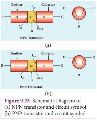
The three regions formed are called as
emitter, base and collector which are provided with terminals or ohmic contacts
labeled as E, B, and C. As a BJT has two p-n junctions, two depletion layers
are formed across the emitter-base junction (JEB) and collector-base
junction (JCB) respectively. The circuit symbol carries an arrowhead
at the emitter lead pointing from p to n indicating the direction of
conventional current.
Emitter:
The main function of the emitter is to
supply majority charge carriers to the collector region through the base
region. Hence, emitter is more heavily doped than the other two regions.
Base:
Base is very thin (10-6
m) and very lightly doped compared to the other two regions.
Collector:
The main function of collector is to
collect the majority charge carriers supplied by the emitter through the base.
Hence, collector is made physically larger than the other two as it has to
dissipate more power. Its is modarately dopped.
Because of the differing size and
the amount of dopping, the emitter and collector cannot be interchanged.
Transistor Biasing
The application of suitable dc
voltages across the transistor terminals is called biasing.
Different modes of transistor biasing
Forward Active:
In this bias the emitter-base junction
is forward biased and the collector-base junction is reverse biased. The
transistor is in the active mode of operation. In this mode, the transistor
functions as an amplifier.
Saturation:
Here, the emitter-base junction and
collector-base junction are forward biased. The transistor has a very large
flow of currents across the junctions. In this mode, transistor is used as a
closed switch.
Cut-off:
In this bias, the emitter-base
junction and collector-base junction are reverse biased. Transistor in this
mode is an open switch.
In a PNP transistor, base and collector
will be negative with respect to emitter indicated by the middle letter N
whereas base and collector will be positive in an NPN transistor [indicated by
the middle letter P]
Transistor circuit configurations
There are three types of circuit
connections for operating a transistor based on the terminal that is used in
common to both input and output circuits.
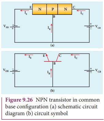
Common-Base(CB) configuration
The base is common to both the input
and output circuits. The schematic and circuit symbol are shown in Figure 9.26(a)
and 9.26(b). The input current is the emitter
current IE and the output current is the collector current IC.
The input signal is applied between emitter and base, the output is measured
between collector and base.
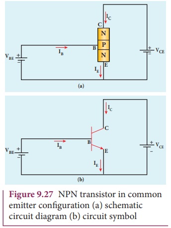
Common-Emitter(CE) configuration
In this configuration, the emitter is common to
both the input and output loops as shown in Figure 9.27. Base current, IB
is the input current and the collector current, IC is the output
current. The input signal is applied between the emitter and base and the
output is measured between the collector and the emitter.
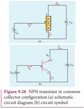
Common-Collector(CC) configuration
Here, the collector is common to
both the input and output circuits as shown in Figure 9.28. The base current IB
is the input current, the emitter current IE is the output current.
The input signal is applied between the base and the collector, the output is measured
between the emitter and collector.
As the output is taken from the
emitter in common collector configuration, it is called an emitter follower.
Related Topics