Chapter: Embedded Systems
Embedded Systems: Memory Testing
EMBEDDED
SYSTEMS: MEMORY TESTING
Unit
Structure
Objectives
1. Introduction
2. Memory Testing and its purpose
3. Common Memory Problems
4. A strategy for memory testing
4.1 Data
Bus Test
4.2 Address
Bus Test
4.3 Device
Test
OBJECTIVES
After reading this chapter you will be able to
understand:
What is memory testing?
What are the common memory related problems?
What are the different types of test to detect
memory related problems and a general idea about the working of these tests
The previous chapter dealt with the different
types of memory. This chapter will focus on the concept of testing memory
devices, its purpose and different methods available.
2 MEMORY
TESTING AND ITS PURPOSE
The purpose of a memory test is to confirm that each storage location in a memory device is working.
Memory Testing is performed when prototype hardware is ready and the designer needs to verify that address and data lines are correctly wired and memory chips are working properly.
Basic idea implement in testing can be understood by this simple task:
Write some set of Data values to each Address in Memory and Read it back to verify.
Ex. If number ’50’ is stored at a particular Address it is expected to be there unless rewritten or erased.
If all values are verified by reading back then Memory device passes the test.
Only through careful selection of data values can make sure passing result to be meaningful.
Difficulties involved in memory testing:
It can be difficult to detect all memory problems with a simple test.
Many Embedded Systems include Memory Tests only to detect catastrophic memory failures which might not even notice memory chips removal.
3 COMMON
MEMORY PROBLEMS
Memory Problems rarely
occur with the chip itself, but due to a variety of post production tests to
check quality this possibility is ruled out.
Catastrophic Failure
is a memory problem that occurs due to physical and electrical damage, it is
uncommon and easily detectable.
A common source of
memory problems is associated with the circuit board. Typical circuit board
problems are:
Circuit
board wiring between Processor & Memory device.
Missing
Memory chip.
Improperly
inserted Memory chip.
Circuit board wiring between Processor & Memory device.
These are usually
caused by,
An error
in design
An error
in production of the board
Any damage
after manufacture
Wires
that connect the memory are:-
i. Address
line :-
select the memory location
ii. Data
line :- transfer
the data
iii. Control
line :- read or write operation
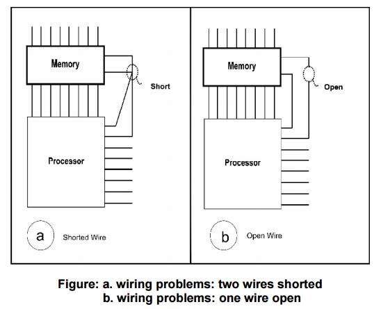
Two
wiring problems are shown below
Connected
to another wire on the board
- May be caused by a bit of solder splash
2.
Not connected to anything
- Caused by broken trace

When Address
line has a wiring problem o
memory locations overlap
o i.e. memory device to see an address different
from the one selected by the processor.
o
Problem is with a data line
o
several data bits “stuck together”
o
i.e. two or more bits always contains same value
When the problem is with a Data line o several data bits “stuck together”
o i.e. two or more bits always contains same value o When Control lines is shorted or open
When Control
lines is shorted or open
o The operation of many control lines is specific to
the processor or memory architecture.
o
the memory will probably not work at all.
2.
Missing Memory chip.
A missing memory chip is clearly a problem that
should be detected
o Unfortunately,
because of the capacitive nature of unconnected electrical wires, some memory
tests will not detect.
For e.g.
suppose you decided to use the following test algorithm write the value 1 to the first location in memory, verify the value by
reading it back write 2 to the second location, verify the value write 3 to the third location, verify, etc.
o Because each read occurs immediately after the
corresponding write, it is possible that the data read back represents nothing
more than the voltage remaining on
the data bus from the previous write.
If the
data is read back too quickly, it will appear that the data has been correctly
stored in memory-even though there is no memory chip at the other end of the
bus!
To detect a missing memory chip the previous
algorithm for test must be altered.
For
example,
write the value
1 to the first location,
2 to the
second location,
And 3 to
the third location,
Then
verify the data at the first location, the second location, etc. If the data
values are unique (as they are in the test just described), the missing chip
will be detected
Improperly inserted Memory chip.
Caused by pins on the
memory chip
o Will either not be connected to the socket at all o Will be connected at the wrong place
Symptoms :-
o System behaves same as though there is a wiring problem or a missing chip.
How to detect :-
o
Detected by any test
4 A
STRATEGY FOR MEMORY TESTING
For memory testing the strategy adopted should
be effective and efficient. Ideally there should be multiple small tests
instead of one large test.
It would be best to have three individual memory
tests:
A
data bus test: Checks
electrical wiring problems
An address bus test: Checks improperly inserted chips
A device test: Checks to detect missing chips and catastrophic failures and problems
with the control bus wiring
These tests have to be executed in a proper
order which is: data bus test first, followed by the address bus test, and then
the device test. That's because the address bus test assumes a working data
bus, and the device test results are meaningless unless both the address and
data buses are known to be good.
4.1
Data Bus Test
It is used to check
data bus wiring.
In this test we need
to confirm that the received data is same as the data sent by processor
Implementation:
Here we
write all possible data values and verify that the memory device stores each
one successfully.
In short
to test the bus one bit at a time.
Walking 1's test
This test
is used to independently test every bit.
A single
data bit is set to 1 and “walked” through the entire data word.
If the data
bus is working properly, the function will return 0.
Otherwise
it will return the data value for which the test failed.
Because we
are testing only the data bus at this point, all of the data values can be written
to the same address. Any address within the memory device will do
00000001
00000010
00000100
00001000
00010000
00100000
01000000
10000000
Figure:
Consecutive data values for walking 1's test
4.2
Address Bus Test
Address bus problems lead to overlapping memory
locations.
In the Address Bus test we need to confirm that
each of the address pins can be set to 0 and 1 without affecting any of the
others.
The smallest set of address that will cover all possible combinations is
the set of “power of two” addresses.
After writing one of the addresses, we must
check none of the others has been overwritten.
4.3
Device Test
It is used to test if the memory device is working properly. It is necessary to test the integrity of the memory device itself.
The thing to test is that every bit in the device is capable of holding both 0 and 1.
For a thorough and complete device test every memory location has to be visited twice.
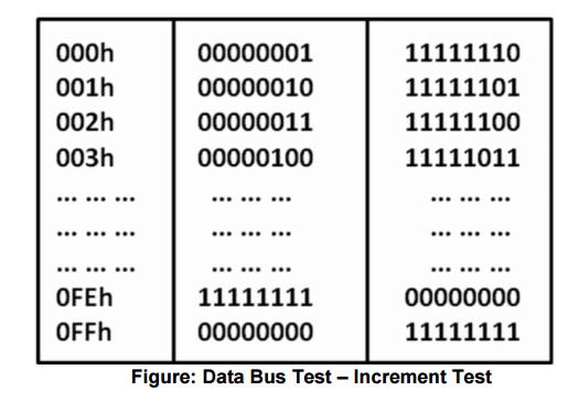
A simple test implemented is the Increment test as shown in the table below
The first column represents the memory location
The second column represents the data that is written at the memory location indicated in column 1 in incremental fashion.
The third column represents the data of column 2 in inverted format.

During the first pass the data in column 1 is verified and during second pass the data in column 2 is verified.
Related Topics