Chapter: Embedded Systems Design : Embedded processors
Motorola MC68000 and its hardware
Motorola MC68000
The MC68000 was a complete design from scratch with the emphasis on
providing an architecture that looked forward with-out the restrictions of
remaining compatible with past designs. Unlike the Intel approach of taking an
8 bit architecture and developing it further and further, Motorola's approach
was to design a 16/32 bit processor whose architecture was more for-ward
looking.
The only support for the old MC6800 family was a hard-ware interface to
allow the new processor to use the existing M6800 peripherals while new M68000
parts were being designed.
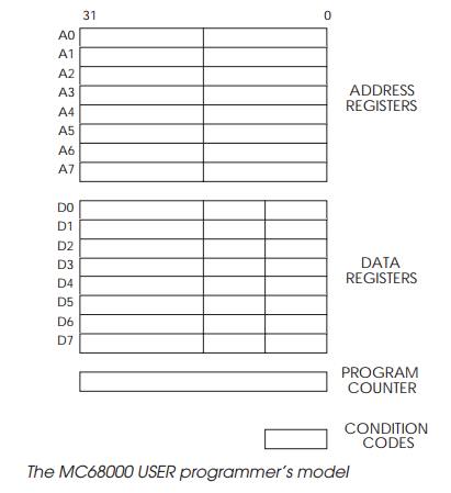
Its design took many of the then current mini and main-frame computer
architectural concepts and developed them using VLSI silicon technology. The
programmer’s register model shows how dramatic the change was. Gone are the
dedicated 8 and 16 bit registers to be replaced by two groups of eight data
registers and eight address registers. All these registers and the program
coun-ter are 32 bits wide.
The MC68000 hardware
Address bus
The address bus (signals A1 – A23) is non-multiplexed and 24 bits wide,
giving a single linear addressing space of 16 Mbytes. A0 is not brought out
directly but is internally decoded to generate upper and lower data strobes.
This allows the processor to access either or both the upper and lower bytes
that comprise the 16 bit data bus.
Data bus
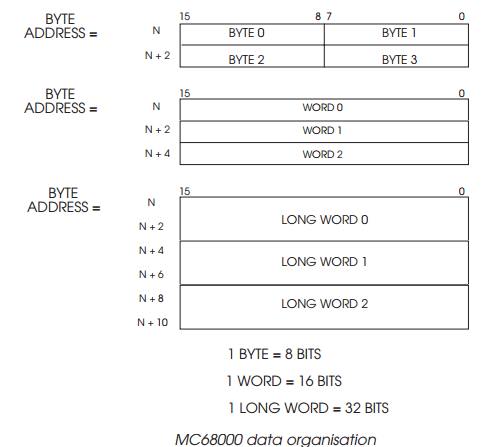
The data bus, D0 – D15, is also non-multiplexed and pro-vides a 16 bit
wide data path to external memory and peripherals. The processor can use data
in either byte, word (16 bit) or long word (32 bit) values. Both word and long
word data is stored on the appropriate boundary, while bytes can be stored
anywhere. The diagram shows how these data quantities are stored. All addresses
specify the byte at the start of the quantity.
If an instruction needs 32 bits of data to be accessed in external
memory, this is performed as two successive 16 bit accesses automatically.
Instructions and operands are always 16 bits in size and accessed on word
boundaries. Attempts to access instructions, operands, words or long words on
odd byte bounda-ries cause an internal ‘address’ error.
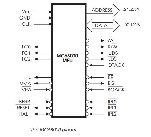
Function codes
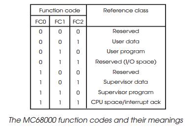
The function codes, FC0–FC2, provide extra information describing what
type of bus cycle is occurring. These codes and their meanings are shown in the
table below. They appear at the same time as the address bus data and indicate
program/data and supervisor/user accesses. In addition, when all three signals
are asserted, the present cycle is an interrupt acknowledgement, where an
interrupt vector is passed to the processor. Many design-ers use these codes to
provide hardware partitioning.
Interrupts
Seven interrupt levels are supported and are encoded on to three
interrupt pins IP0–IP2. With all three signals high, no exter-nal interrupt is
requested. With all three asserted, a non-maskable level 7 interrupt is
generated. Levels 1–6, generated by other combinations, can be internally
masked by writing to the appro-priate bits within the status register.
The interrupt cycle is started by a peripheral generating an interrupt.
This is usually encoded using a 148 priority encoder. The appropriate code
sequence is generated and drives the inter-rupt pins. The processor samples the
levels and requires the levels to remain constant to be recognised. It is
recommended that the interrupt level remains asserted until its interrupt acknowledge-ment
cycle commences to ensure recognition. Once the processor has recognised the
interrupt, it waits until the current instruction has been completed and starts
an interrupt acknowledgement cycle. This starts an external bus cycle with all
three function codes driven high to indicate an interrupt acknowledgement
cycle.
The interrupt level being acknowledged is placed on ad-dress bus bits
A1–A3 to allow external circuitry to identify which level is being
acknowledged. This is essential when one or more interrupt requests are
pending. The system now has a choice over which way it will respond:
•
If the peripheral can generate an
8 bit vector number, this is placed on the lower byte of the address bus and
DTACK* asserted. The vector number is read and the cycle com-pleted. This
vector number then selects the address and subsequent software handler from the
vector table.
•
If the peripheral cannot generate
a vector, it can assert VPA* and the processor will terminate the cycle using the
M6800 interface. It will select the specific interrupt vector allocated to the
specific interrupt level. This method is called auto-vectoring.
To prevent an interrupt request generating multiple ac-knowledgements,
the internal interrupt mask is raised to the interrupt level, effectively
masking any further requests. Only if a higher level interrupt occurs will the
processor nest its interrupt service routines. The interrupt service routine
must clear the interrupt source and thus remove the request before returning to
normal execution. If another interrupt is pending from a different source, it
will be recognised and cause another acknowledgement to occur.
Error recovery and control signals
There are three signals associated with error control and recovery. The
bus error BERR*, HALT* and RESET* signals can provide information or be used as
inputs to start recovery proce-dures in case of system problems.
The BERR* signal is the counterpart of DTACK*. It is used during a bus
cycle to indicate an error condition that may arise through parity errors or
accessing non-existent memory. If BERR* is asserted on its own, the processor
halts normal processing and goes to a special bus error software handler. If
HALT* is asserted at the same time, it is possible to rerun the bus cycle.
BERR* is removed followed by HALT* one clock later, after which the previous
cycle is rerun automatically. This is useful to screen out transient errors.
Many designs use external hardware to force a rerun automatically but will cause
a full bus error if an error occurs during the rerun.
Without such a signal, the only recourse is to complete the transfer,
generate an immediate non-maskable interrupt and let a software handler attempt
to sort out the mess! Often the only way out is to reset the system or shut it
down. This makes the system extremely intolerant of signal noise and other such
transient errors.
The RESET* and HALT* signals are driven low at power-up to force the
MC68000 into its power-up sequence. The operation takes about 100 ms, after
which the signals are negated and the processor accesses the RESET vector at
location 0 in memory to fetch its stack pointer and program counter from the
two long words stored there.
Related Topics