Chapter: Embedded Systems Design : Embedded processors
DSP basic architecture
DSP basic architecture
As an example of a powerful DSP processor, consider the Motorola
DSP56000. It is used in many digital audio applications where it acts as a
multi-band graphics equaliser or as a noise reduction system.
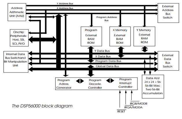
The processor is split into 10 functional blocks. It is a 24 bit data
word processor to give increased resolution. The device has an enhanced Harvard
architecture with three separate external buses: one for program and X and Y
memories for data. The communication between these and the outside world is
controlled by two external bus switches, one for data and the other for
addresses. Internally, these two switches are functionally repro-duced by the
internal data bus switch and the address arithmetic unit (AAU). The AAU
contains 24 address registers in three banks of 8. These are used to reference
data so that it can be easily fetched to maintain the data flow into the data
ALU.
The program address generator, decode controller and interrupt
controller organise the instruction flow through the processor. There are six
24 bit registers for controlling loop counts, operating mode, stack
manipulation and condition codes. The program counter is 24 bit although the
upper 8 bits are only used for sign extension.
The main workhorse is the data ALU, which contains two 56 bit
accumulators A and B which each consist of three smaller registers A0, A1, A2,
B0, B1 and B2. The 56 bit value is stored with the most significant 24 bit word
in A1 or B1, the least significant 24 bit word in A0 or B0 and the 8 bit
extension word is stored in A2 or B2. The processor uses a 24 bit word which
can provide a dynamic range of some 140 dB, while intermediate 56 bit results
can extend this to 330 dB. In practice, the extension byte is used for over-
and underflow. In addition there are four 24 bit registers X1, X0, Y1 and Y0.
These can also be paired to form two 48 bit registers X and Y.
These registers can read or write data from their respective data buses
and are the data sources for the multiply–accumulate (MAC) operation. When the
MAC instruction is executed, two 24 bit values from X0, X1, Y1 or Y0 are
multiplied together, and then added or subtracted from either accumulator A or B.
This takes place in a single machine cycle of 75 ns at 27 MHz. While this is
executing, two parallel data moves can take place to update the X and Y
registers with the next values. In reality, four separate operations are taking
place concurrently.
The data ALU also contains two data shifters for bit ma-nipulation and
to provide dynamic scaling of fixed point data without modifying the original
program code by simply program-ming the scaling mode bits. The limiters are
used to reduce any arithmetic errors due to overflow, for example. If overflow
occurs, i.e. the resultant value requires more bits to describe it than are
available, then it is more accurate to write the maximum valid number than the
overflowed value. This maximum or limited value is substituted by the data
limiter in such cases, and sets a flag in the condition code register to
indicate what has happened.
The external signals are split into various groups. There are three
ports A, B and C and seven special bus control signals, two interrupt pins,
reset, power and ground and, finally, clock signals. The device is very similar
in design to an 8 bit microcontroller unit (MCU), and it can be set into
several different memory configura-tions.
The three independent memory spaces, X data, Y data and program are
configured by the MB, MA and DE bits in the operating mode register. The MB and
MA bits are set according to the status of the MB and MA pins during the
processor´s reset sequence. These pins are subsequently used for external
inter-rupts. Within the program space, the MA and MB bits determine where the
program memory is and where the reset starting ad-dress is located. The DE bit
either effectively enables or disables internal data ROMs which contain a set
of µ and A Law expansion tables in the X data ROM and a four quadrant sine
wave table in the Y data ROM. The on-chip peripherals are mapped into the X
data space between $FFC0 and $FFFF. Each of the three spaces is 64 kbytes in
size.
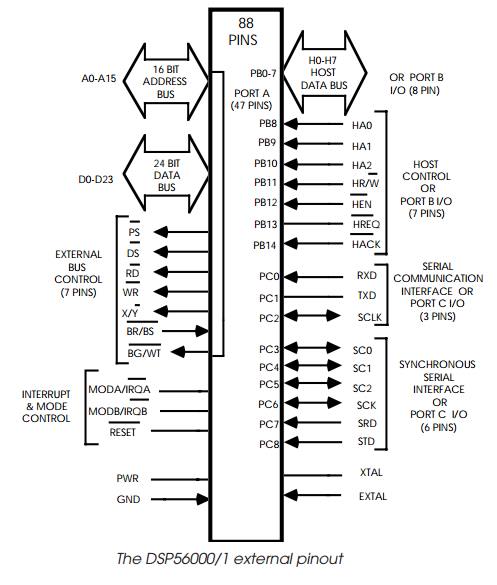
These memory spaces communicate to the outside world via a shared 16 bit
address bus and a 24 bit data bus. Two additional signals, PS* and X/Y*
identify which type of access is taking place. The DSP56000 can be programmed
to insert a fixed number of wait states on external accesses for each memory
space and I/O. Alternatively, an asynchronous handshake can be adopted by using
the bus strobe and wait pins (BS* and WT*).
Using a DSP as a microcontroller is becoming another common trend. The
processor has memory and peripherals which makes it look like a microcontroller
— albeit one with a very fast processing capability and slightly different
programming tech-niques. This, coupled with the increasing need for some form
of DSP function such as filtering in many embedded systems, has meant that DSP
controllers are a feasible choice for embedded designs.
Related Topics