Chapter: Embedded Systems Design : Embedded processors
Motorola MC68030
Motorola MC68030
The MC68030 appeared some 2–3 years after the MC68020 and used the
advantage of increased silicon real estate to integrate more functions on to a
MC68020-based design. The differences between the MC68020 and the MC68030 are
not radical — the newer design can be referred to as evolutionary rather than a
quantum leap. The device is fully MC68020 compatible with its full instruction
set, addressing modes and 32 bit wide register set. The initial clock frequency
was designed to 20 MHz, some 4 MHz faster than the MC68020, and this has
yielded commercially available parts running at 50 MHz. The transistor count
has increased to about 300000 but with smaller geometries; die size and heat
dissipation are similar.
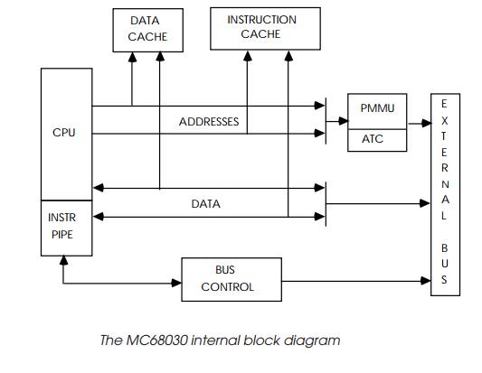
Memory management has now been brought on-chip with the MC68030 using a
subset of the MC68851 PMMU with a smaller 22 entry on-chip address translation
cache. The 256 byte instruc-tion cache of the MC68020 is still present and has
been augmented with a 256 byte data cache.
Both these caches are logical and are organised differently from the 64 × 4 MC68020 scheme. A 16 × 16 organisation has been adopted
to allow a new synchronous bus to burst fill cache lines. The cache lookup and
address translations occur in parallel to improve performance.

The processor supports both the coprocessor interface and the MC68020
asynchronous bus with its dynamic bus sizing and misalignment support. However,
it has an alternative synchro-nous bus interface which supports a two–clock
access with op-tional single-cycle bursting. The bus interface choice can be
made dynamically by external hardware.
Related Topics