Chapter: Embedded Systems Design : Embedded processors
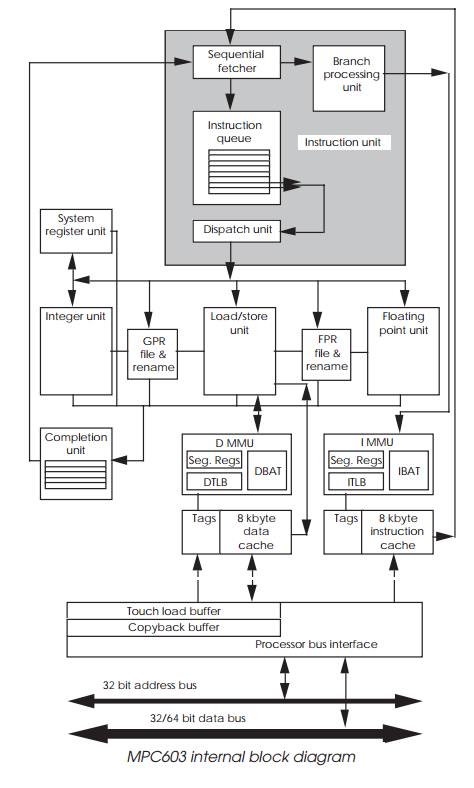
The MPC603 block diagram
The MPC603 block diagram
The MPC603 was the second PowerPC processor to appear. Like the MPC601,
it has the three execution units: a branch unit to resolve branch instructions,
an integer unit and a floating point unit.
The floating point unit supports IEEE format. However, two additional execution
units have been added to provide dedi-cated support for system registers and to
move data between the register files and the two on-chip caches. The processor
is superscalar and can dispatch up to three instructions and process five every
clock cycle.
The branch unit supports both branch folding and specula-tive execution.
It augments this with register renaming, which allows speculative execution to
continue further than allowed on the MPC601 and thus increase the processing
advantages of the processor.

The general-purpose register file consists of 32 separate registers,
each 32 bits wide. The floating point register file contains 32 registers, each
64 bits wide to support double precision floating point. The external physical
memory map is a 32 bit address linear organisation and is 4 Gbytes in size.
The MPC603’s memory subsystem consists of a separate memory management
unit and on-chip cache for data and instruc-tions which communicates to
external memory via a 32 bit address bus and a 64 or 32 bit data bus. This bus
can, at its peak, fetch two instructions per clock or 64 bits of data. Each
cache is 8 kbytes in size, giving a combined on-chip cache size of 16 kbytes.
The bus also supports split transactions, where the address bus can be used
independently and simultaneously with the data bus to improve its utilisation.
Bus snooping is also provided to ensure cache coherency with external memory.
As with the MPC601, the MPC603 speeds up the address translation
process, by keeping translation information in one of four translation
lookaside buffers, each of which is divided into two pairs, one for data
accesses and the other for instruction fetches. It is different from the MPC601
in that translation tablewalks are performed by the software and not
automatically by the processor.
The device also includes power management facilities and is eminently
suitable for low power applications.
Related Topics