Chapter: Embedded Systems Design : Embedded processors
Example 8 bit architectures: Z80, Z80 programming model, MC6800
Example 8 bit architectures
Z80
The Z80 microprocessor is an 8 bit CPU with a 16 bit address bus capable
of direct access to 64k of memory space. It was designed by Zilog and rapidly
gained a lot of interest. The Z80 was based on the Intel 8080 but has an
extended instruction set and many hardware improvements. It can run 8080 code
if needed by its support of the 8080 instruction set. The instruction set is
essential based around an 8 bit op code giving a maximum of 256 instructions.
The 158 instructions that are specified — the others are reserved — include 78
instructions from the 8080. The instruc-tion set supports the use of extension
bytes to encode additional information. In terms of processing power, it
offered about 1 MIP at 4 MHz clock speed with a minimum instruction time of 1 µs and a
maximum instruction time of 5.75 µs.


The programming model includes an accumulator and six 8 bit registers
that can be paired together to create three 16 bit registers. In addition to
the general registers, a stack pointer, program counter, and two index (memory
pointers) registers are provided. It uses external RAM for its stack. While not
as powerful today as a PowerPC or Pentium, it was in its time a very powerful
processor and was used in many of the early home computers such as the Amstrad
CPC series. It was also used in many embedded designs partly because of its
improved performance and also for its built-in refresh circuitry for DRAMs.
This circuitry greatly simplified the external glue logic that was needed with
DRAMs.
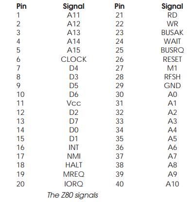
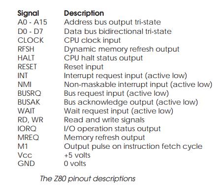
The Z80 was originally packaged in a 40 pin DIP package and ran at 2.5
and 4 MHz. Since then other packages and speeds have become available including
low power CMOS versions — the original was made in NMOS and dissipated about 1
watt. Zilog now use the processor as a core within its range of Z800
microcontrollers with various configurations of on-chip RAM and
EPROM.
Z80 programming model
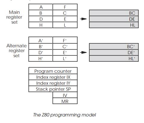
The Z80 programming model essential consists of a set of 8 bit registers
which can be paired together to create 16 bit versions for use as data storage
or address pointers. There are two register sets within the model: the main and
alternate. Only one set can be used at any one time and the switch and data
transfer is performed by the EXX instruction. The registers in the alternate
set are designated by a ´ suffix.

The model has an 8 bit accumulator A and a flags register known as F.
This contains the status information such as carry, zero, sign and overflow.
This register is also known as PSW (program status word) in some documentation.
Registers B, C, D, E, H and L are 8 bit general-purpose registers that can be
paired to create 16 registers known as BC, DE and HL. The remaining registers
are the program counter PC, two index registers IX and IY and a stack pointer
SP. All these four registers are 16 bits in size and can access the whole 64
kbytes of external memory that the Z80 can access. There are two additional
registers IV and MR which are the interrupt vector and the memory refresh
registers. The IV register is used in the interrupt handling mode 2 to point to
the required software routine to process the interrupt. In mode 1, the
interrupt vector is supplied via the external data bus. The memory refresh
register is used to control the on-chip DRAM refresh circuitry.
Unlike the MC6800, the Z80 does not use memory mapped I/O and instead
uses the idea of ports, just like the 8080. The lower 8 bits of the address bus
are used along with the IORQ signal to access any external peripherals. The
IORQ signal is used to differ-entiate the access from a normal memory cycle.
These I/O accesses are similar from a hardware perspective to a memory cycle
but only occur when an I/O port instruction (IN, OUT) is executed. In some
respects, this is similar to the RISC idea of load and store instructions to
bring information into the processor, process it and then write out the data.
This system gives 255 ports and is usually sufficient for most embedded
designs.
MC6800
The MC6800 was introduced in the mid-1970s by Motorola and is as an architecture
the basis of several hundred derivative processors and microcontrollers such as
the MC6809, MC6801, MC68HC05, MC68HC11, MC68HC08 families.
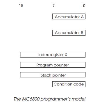
The processor architecture is 8 bits and uses a 64 kbyte memory map. Its
programming model uses two 8 bit accumula-tors and a single 16 bit index
register. Later derivatives such as the MC68HC11 added an additional index
register and allowed the two accumulators to be treated as a single 16 bit
accumulator to provide additional support for 16 bit arithmetic.

Its external bus was synchronous with separate address and data ports
and the device operated at either 1, 1.5 or 2 MHz. The instruction set was
essentially based around an 8 bit instruc tion with extensions for immediate
values, address offsets and so on. It supported both non-maskable and software
interrupts.
These type of processors have largely been replaced today by the
microcontroller versions which have the same or advanced processor
architectures and instruction sets but have the added advantage of glueless
interfaces to memory and peripherals incor-porated onto the chip itself.
Discrete processors are still used but these tend to be the higher performance
devices such as the MC68000 and 80x86 processors. But even with these faster
and higher performance devices, the same trend of moving to inte-grated
microcontroller type of devices is being followed as even higher performance
processors such as RISC devices become available.
Related Topics