Chapter: Embedded Systems Design : Embedded processors
Intel Pentium
Intel Pentium
The Pentium is essentially an enhanced 80486 from a programming model.
It uses virtually the same programming model and instruction set — although
there are some new additions.
The most noticeable enhancement is its ability to operate as a
superscalar processor and execute two instructions per clock. To do this it has
incorporated many new features that were not present on the 80486.
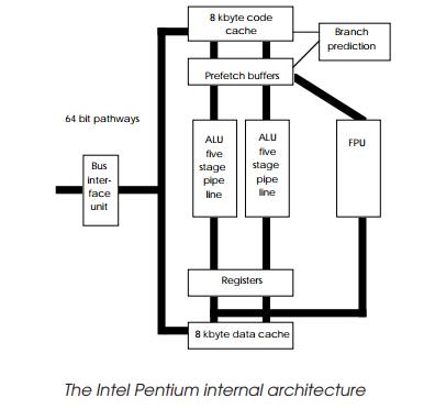
As the internal architecture diagram shows, the device has two
five-stage pipelines that allow the joint execution of two integer instructions
provided that they are simple enough not to use microcode or have data
dependencies. This restriction is not that great a problem as many compilers
have now started to concentrate on the simpler instructions within CISN
instruction sets to improve their performance.
To maintain the throughput, the unified cache that ap-peared on the
80486 has been dropped in favour of two separate 8 kbyte caches: one for data
and one for code. These caches are fed by an external 64 bit wide burst mode
type data bus. The caches also now support write-back MESI policies instead of
the less efficient write-through design.
Branches are accelerated using a branch target cache and work in
conjunction with the code cache and prefetch buffers. The instruction set now
supports an 8 byte compare and exchange instruction and a special processor
identification instruction. The cache coherency support also has some new
instructions to allow programmer’s control of the MESI coherency policy.

The Pentium has an additional control register and system management
mode register that first appeared on the 80386SL which provides intelligent
power control.

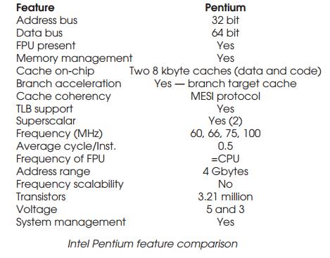
Feature Pentium
Address bus 32
bit
Data bus 64 bit
FPU present Yes
Memory management Yes
Cache on-chip Two 8 kbyte
caches (data and code)
Branch acceleration Yes
— branch target cache
Cache coherency MESI
protocol
TLB support Yes
Superscalar Yes (2)
Frequency (MHz) 60, 66,
75, 100
Average cycle/Inst. 0.5
Frequency of FPU =CPU
Address range 4
Gbytes
Frequency scalability No
Transistors 3.21 million
Voltage 5 and 3
System management Yes
Pentium Pro
The Pentium Pro processor is the name for Intel's successor to the
Pentium and was previously referred to as the P6 processor. The processor was
Intel’s answer to the RISC threat posed by the DEC Alpha and Motorola PowerPC
chips. It embraces many techniques that are used to achieve superscalar
performance that have appeared previously on RISC processors such as the MPC604
PowerPC chip. It was unique in that the device actually consisted of two
separate die within a single ceramic pin grid array: one die is the processor
with its level one cache on-chip and the second die is the level 2 cache which
is needed to maintain the instruction and data throughput needed to maintain
the level of performance. It was originally introduced at 133 MHz and gained
some accept-ance within high-end PC/workstation applications. Both caches
support the full MESI cache coherency protocol.
It achieves superscalar operation by being able to execute up to five
instructions concurrently although this is a peak figure and a more realistic
one to two instructions per clock is a more accurate average figure. This is
done through a technique called dynamic execution using multiple branch
prediction, dataflow analysis and speculative execution.
Multiple branch prediction
This is where the processor predicts where a branch instruc-tion is
likely to change the program flow and continues execution based on this
assumption, until proven or more accurately, until correctly evaluated. This
removes any delay providing the branch prediction was correct and speeds up
branch execution.
Data flow analysis
This is an out of order execution and involves analysing the code and
determining if there are any data dependencies. If there are, this will stall
the superscalar execution until these are re-solved. For example, the processor
cannot execute two consecu-tive integer instructions if the second instruction
depends on the result of its predecessor. By internally reordering the
instructions, such delays can be removed and thus faster execution can be
restored. This can cause problems with embedded systems in that the reordering
means that the CPU will not necessarily execute the code in programme order but
in a logical functional sequence. To do this, the processor needs to understand
any restrictions that may affect its reordering. This information is frequently
provided by splitting the memory map into areas, with each area having its own
attributes. These functions are described in Chapter 3.
Speculative execution
Speculative execution is where instructions are executed speculatively,
usually following predicted branch paths in the code until the true and correct
path can be determined. If the processor has speculated correctly, then
performance has been gained. If not, the speculative results are discarded and
the proc-essor continues down the correct path. If more correct speculation is
achieved than incorrect, the processor performance increases.
It is fair to say that the processor has not been as successful as the
Pentium. This is because faster Pentium designs, especially those from Cyrix,
outperformed it and were considerably cheaper. The final problem it had was
that it was not optimised for 16 bit software such as MS-DOS and Windows 3.x
applications and required 32 bit software to really achieve its performance.
The delay in the market in getting 32 bit software — Windows 95 was almost 18
months late and this stalled the market considerably — did not help its cause,
and the part is now overshadowed by the faster Pentium parts and the Pentium
II.
The MMX instructions
The MMX instructions or multimedia extensions as they have also been
referred to were introduced to the Pentium proces-sor to provide better support
for multimedia software running on a PC using the Intel architecture. Despite
some over-exaggerated claims of 400% improvement, the additional instructions
do pro-vide additional support for programmers to improve their code. About 50
instructions have been added that use the SIMD (single instruction, multiple
data) concept to process several pieces of data with a single instruction,
instead of the normal single piece of data.
To do this, the eight floating point registers can be used to support
MMX instructions or floating point. These registers are 80 bits wide and in
their MMX mode, only 64 bits are used. This is enough to store a new data type
known as the packed operand. This supports eight packed bytes, four packed 16
bit words, two packed 32 bit double words, or a single 64 bit quad word. This
is extremely useful for data manipulation where pixels can be packed into the
floating point register and manipulated simultaneously.
The beauty of this technique is that the basic architecture and register
set does not change. The floating point registers will be saved on a context
switch anyway, irrespective of whether they are storing MMX packed data or
traditional floating point values. This is where one of the problems lies. A
program can really only use floating point or MMX instructions. It cannot mix
them without clearing the registers or saving the contents. This is because the
floating point and MMX instructions share the same registers.
This has led to problems with some software and the discovery of some
bugs in the silicon (run a multimedia applica-tion and then watch Excel get all
the financial calculations wrong). There are fixes available and this problem
has been resolved. However, the success of MMX does seem to be dependent on
factors other than the technology and the MMX suffix has become a requirement.
If a PC doesn’t have MMX, it is no good for multimedia. For embedded system,
this statement is not valid and its use is not as obligatory as it might seem.
What is interesting is that MMX processors also have other improvements
to help the general processor performance and so it can be a little difficult
to see how much MMX can actually help. The second point is that many RISC
processors, especially the PowerPC as used in the Apple Macintosh, can beat an
MMX processor running the same multimedia application. The reason is simple.
Many of the instructions and data manipulation that MMX brings, these
processors have had as standard. They may not have packed data, but they don’t
have to remember if they used a floating point instruction recently and should
now save the regis-ters before using an MMX instruction. What seems to be an elegant
solution does have some drawbacks.
The Pentium II
The Pentium II was the next generation Intel processor and uses a module
based technology and a PCB connector to provide the connection to a Intel
designed motherboard. It no longer uses a chip package and is only available as
a module. Essentially, a redesigned and improved Pentium Pro core with larger
caches, it was the fastest Intel processor available until the Pentium III
appeared. It is clear that Intel is focusing on the PC market with its 80x86
architecture and this does raise the question the suitability of these
processors to be used in embedded systems. With the subsequent Pentium III and
Pentium IV processors requiring specialised motherboard support, their
suitability for embedded designs is limited to completely built boards and
hardwares. The other problem with these types of architectures is that the
inte-grated caches and other techniques they use to get the processing speed
mean that the processor becomes more statistical in nature and it becomes
difficult to predict how long it will take to do a task. This is another topic
we will come back to in later chapters.
Related Topics