Chapter: Embedded Systems
Embedded Hardware from Software Programmers Perspective
EMBEDDED
HARDWARE FROM SOFTWARE PROGRAMMERS PERSPECTIVE
Unit
Structure
Objectives
1. Introduction
2. Components on an embedded system
3. Memory Map
4. I/O Map
5. Interrupt Map
OBJECTIVES
After reading this chapter you will be able to:
Understand in general the difference in
programming software for general purpose computers and embedded systems
The way in which processor communicates with
components of embedded system
Memory Map, I/O Map & Interrupt Map
1
INTRODUCTION
The software programmer must know the hardware
involved in an embedded system before he can even attempt to write code for its
functioning.
Programming for embedded systems is different
than programming on computers. Embedded systems have certain strict assumptions
to be followed. Until the programmer does not know what hardware components are
involved and what are the assumptions and rules related to those components,
the program or code cannot be written.
This chapter introduces the reader with the
hardware of embedded system from a software perspective. It is this where the
reader shall understand where the code fits in an embedded system.
2
COMPONENTS ON AN EMBEDDED SYSTEM
Before
the programmer can start to code anything, he has to invest some time in
understand the functioning of the embedded system.
He is expected to understand the following
things:
Functioning or purpose of the embedded system
Individual components involved
The way data flows through the components of an
embedded system.
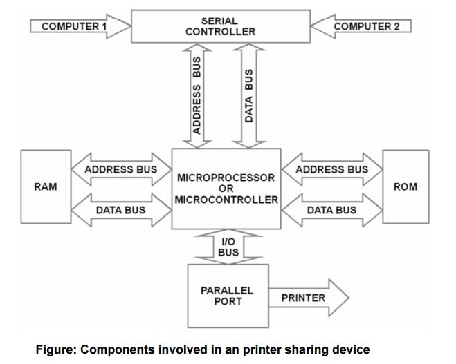
Consider
an example of an embedded system intended to be used as a printer-sharing
device. This device is attached to a printer and allows access to two computers
through serial interface and one printer through a parallel interface.
The
diagram below describes the way the devices are connected to each other. Data
to be printed is accepted from either serial port, held in RAM until the
printer is ready for more data, and delivered to the printer via the parallel
port. The software that makes all of this happen is stored in ROM.
The
working or execution of the code is brought about by the processor. The
processor knows two types of components: memory and peripherals.
Memories are for data and code storage and
retrieval. Ex.
RAM & ROM
Peripherals are specialized hardware devices
that either coordinate interaction with the outside world (I/O) or perform a
specific hardware function. Ex. Serial Port
Certain
processors like intel communicate with these memories and peripherals with two
distinct address spaces.
The
first address space is called the memory space and is intended mainly for
memory devices; the second is reserved exclusively for peripherals and is
called the I/O space.
When
peripherals are located in I/O space they are called I/O Mapped peripheral else
when peripherals are located in memory space they are called Memory Mapped
peripherals or memory mapped I/O.
If given a choice, Memory mapped peripherals are
better because it has advantages for both the hardware and software developers.
It is attractive to the hardware developer because he might be able to
eliminate the I/O space, and some of its associated wires, altogether. It is
attractive to the software developer who is able to use pointers, data
structures, and unions to interact with the peripherals more easily and
efficiently.
3
MEMORY MAP
A Memory Map is the
processor's "address book." It shows what these devices look like to the
processor. The memory map contains one entry for each of the memories and
peripherals that are accessible from the processor's memory space.
All processors store
their programs and data in memory.
These chips are
located in the processor's memory space, and the processor communicates with
them by way of two sets of electrical wires called the address bus and the data
bus. To read or write a particular location in memory, the processor first
writes the desired address onto the address bus. The data is then transferred
over the data bus.
A memory map is a
table that shows the name and address range of each memory device and
peripheral that is located in the memory space.
Organize the table
such that the lowest address is at the bottom and the highest address is at the
top. Each time a new device is added, add it to the memory map, place it in its
approximate location in memory and label the starting and ending addresses, in
hexadecimal. After inserting all of the devices into the memory map, be sure to
label any unused memory regions as such.
The block diagram of
the Printer sharing device shown above contains three devices attached to the
address and data buses. These devices are the RAM and ROM and a Serial
Controller.
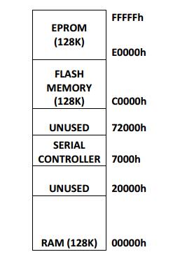
Let us assume that the
RAM is located at the bottom of memory and extends upward for the first 128 KB
of the memory space.
The ROM is located at
the top of memory and extends downward for 256 KB. But considering the ROM
contains two ROMs-an EPROM and a Flash memory device-each of size 128 KB.
The third device, the
Serial Controller, is a memory-mapped peripheral whose registers are accessible
between the addresses say 70000h and 72000h.
The
diagram below shows the memory map for the printer sharing device.
For every embedded system, a header file should
be created that describes these important features and provides an abstract
interface to the hardware. It allows the programmer to refer to the various
devices on the board by name, rather than by address.
The part of the header
file below describes the memory map
#define
RAM_BASE (void *) 0x00000000
#define
SC_BASE (void *) 0x70000000
#define
SC_INTACK (void *) 0x70001000
#define
FLASH_BASE (void *) 0xC0000000
#define
EPROM_BASE (void *) 0xE0000000
4 I/O
MAP
The I/O map contains one entry for each of the
peripheral.
To create an I/O map, simply create a table of peripheral names and address ranges, organized in such a way that the lowest addresses are at the bottom.
The diagram below shows the I/O map for the printer sharing device
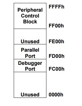
It includes three devices: the peripheral control block (PCB), parallel port, and debugger port. The PCB is a set of registers within the processor that are used to control the on-chip peripherals. The chips that control the parallel port and debugger port reside outside of the processor. These ports are used to communicate with the printer and a host-based debugger, respectively.
The part of the header file below describes the I/O map
#define SVIEW_BASE 0xFC00
#define PIO_BASE 0xFD00
#define PCB_BASE 0xFF00
5
INTERRUPT MAP
There are two techniques which can be used by the processor to
communicate with memories or peripheral devices. These are:
a.
Polling: In this technique
the processor polls the device (asks
question) repeatedly at regular intervals to check if the device has completed
the given task or has any new task to execute.
b. Interrupt:
An
interrupt is a
signal sent from
a peripheral to the
Upon receiving an interrupt signal the Processor does the job by issuing certain commands and waits for another interrupt to signal the completion of the job.
While the processor is waiting for the interrupt to arrive, it is free to continue working on other things.
When a fresh interrupt signal is received, the processor temporarily sets aside its current work and executes a small piece of software called the interrupt service routine (ISR). When the ISR completes, the processor returns to the work that was interrupted.
The programmer must write the ISR himself and enable it so that it will be executed when the relevant interrupt occurs.
Interrupt
Map
Embedded systems usually have only a handful of
interrupts. Associated with each of these are an interrupt pin which is present
on the outside of the processor chip and an ISR.
In order for the processor to execute the correct ISR, a mapping must exist between interrupt pins and ISRs. This mapping usually takes the form of an interrupt vector table.
The vector table is usually just an array of pointers to functions, located at some known memory address. The processor uses the interrupt type (a unique number associated with each interrupt pin) as its index into this array. The value stored at that location in the vector table is usually just the address of the ISR to be executed.
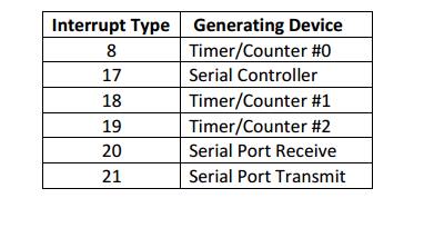
An Interrupt Map is a step taken in this process. The Interrupt Map is a table that contains a list of interrupt types and the devices to which they refer.
The diagram below shows the Interrupt map for the printer sharing device
•Once the I/O map is created the header file should be appended with the following information:
#define SCC_INT 17 /*Serial Controller*/
#define TIMER0_INT 8 /* On-Chip Timer/Counters*/
#define TIMER1_INT 18
#define TIMER2_INT 19
#define RX_INT 20 /* On-Chip Serial Ports */
#define TX_INT 21
Related Topics