Chapter: 11th 12th std standard Class Physics sciense Higher secondary school College Notes
Operational amplifier (OP - AMP)
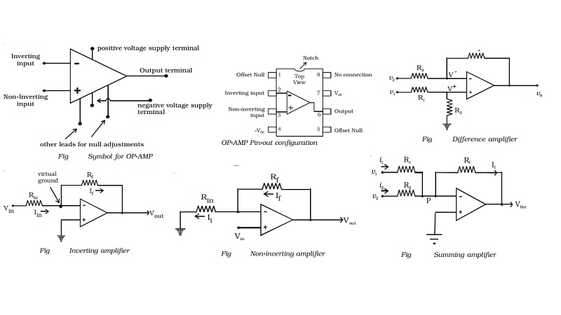
Operational amplifier (OP - AMP)
Linear integrated circuits are
being used in a number of electronic applications, such as in the fields like
communication, medical electronics, instrumentation control etc. An important
linear IC is an operational amplifier.
OP-AMP is a solid state device capable of sensing and amplifying
dc and ac input signals. OP-AMP is an amplifier with two inputs (differential
inputs) and a single output. OP-AMP consists of 20 transistors, 11 resistors
and one capacitor. It usually requires a positive and negative power supply
(dual power supply). This allows the output voltage to swing positive and
negative with respect to ground.
The most important
characteristics of OP-AMP are : (i) very high input impedance or even infinity
which produces negligible current at the inputs, (ii) very high gain, (iii)
very low output impedance or even zero, so as not to affect the output of the
amplifier by loading.
An OP-AMP is so named, because it
was originally designed to perform mathematical operations such as addition,
subtraction, multiplication, division, integration, differentiation etc in
analog computer. Nowdays OP-AMPs are used in analog computer operations and in
timing circuits.
Circuit symbol and Pin-out
configuration of an OP-AMP
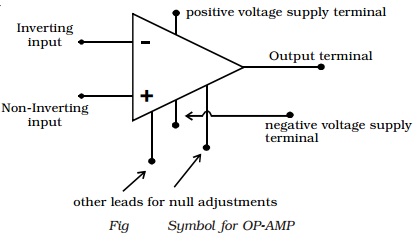
The OP - AMP is represented by a
triangular symbol as shown in Fig. It has two input terminals and one output
terminal. The terminal with negative
sign is called as the inverting input and the terminal with positive sign is called as the
non-inverting input. The input terminals are at the base of the triangle. The
output terminal is shown at the apex of the triangle.
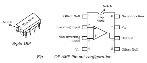
The widely used very popular type
Op-Amp IC 741, which is available in DIP. Referring to the top view of the
dual-in-package, the pin configuration of IC 741 can be described (Fig) as
follows. The top pin on the left side of the notch indicates Pin 1. The pin
number 2 is inverting input terminal and 3 is non-inverting input terminal. Pin
6 is the output terminal. A d.c. voltage or a.c signal placed on the inverting
input will be 180o out of phase at the output. A d.c. voltage or
a.c. signal placed on the non-inverting input will be inphase at the output.
Pins 7 and 4 are the power supply terminals. Terminals 1 and 5 are used for
null adjustment. Null adjustment pins are used to null the output voltage when
equal voltages are applied to the input terminals for perfect balance. Pin 8
indicates no connection.
Basic OP-AMP circuits
This section concentrates on the
principles involved with basic OP-AMP circuit viz, (i) inverting and (ii)
non-inverting amplifiers.
(i) Inverting amplifier
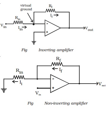
The basic OP-AMP inverting
amplifier is shown in Fig. The input voltage Vin is applied to the
inverting input through the input resistor Rin. The non inverting
input is grounded. The feedback resistor Rf is connected between the
output and the inverting input.
Since the input impedance of an
op-amp is considered very high, no current can flow into or out of the input
terminals. Therefore Iin must flow through Rf and is
indicated by If (the feedback current). Since Rin and Rf
are in series, then Iin = If. The voltage between
inverting and non-inverting inputs
is essentially equal to zero
volt. Therefore, the inverting input terminal is also at 0 volt. For this
reason the inverting input is said to be at virtual ground. The output voltage
(Vout) is taken across Rf.
It can be proved that
If=Vout/Rf
Since Iin =If ,
then
Vin/Rin =
-Vout/Rf
Rearranging the equation, we
obtain
-Vout/Vin =
Rf/Rin
∴ The voltage gain of an inverting amplifier can be expressed as
Av = -Rf/Rin
The amplifier gain is the ratio
of Rf to Rin
Finally, the output voltage can
be found by
Vout = -Rf/Rin
x Vin
The output voltage is out of
phase with the input voltage.
(ii) Non-inverting amplifier
The basic OP-AMP non-inverting
amplifier is shown in Fig. The input signal Vin is applied to the
non-inverting input terminal. The resistor Rin is connected from the
inverting input to ground. The feedback resistor Rf is connected between
the output and the inverting input.
Resistors Rf and Rin
form a resistive ratio network to produce the feedback voltage (VA)
needed at the inverting input. Feedback voltage (VA) is developed
across Rin. Since the potential at the inverting input tends to be
the same as the non-inverting input (as pointed out with the description of
virtual ground), Vin = VA.
Since VA = Vin,
the gain of the amplifer can be expressed as
Av = Vou t
![]() V A
V A
However, VA is
determined by the resistance ratio of Rin and Rf ; thus,
VA=[Rin/(Rf/Rin)]
Vout
Av=1+(Rf/Rin)
Finally, the output voltage can
be found by, Vout = (1+Rf/Rin)Vin
It is seen that the input and
output voltages are in phase
(iii) Summing amplifier
The summing amplifier provides an
output voltage equal to the algebraic sum of the input voltages.
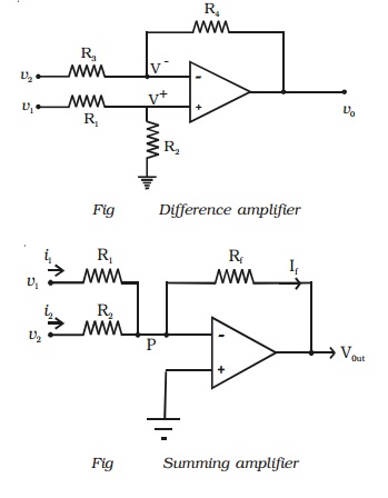
Fig shows an inverting amplifier,
used to sum two input voltages. The input voltages v1 and v2
are applied through the resistors R1 and R2 to the
summing junction (P) and Rf is the feedback resistor. At the point P,
i1 + i2 =if
Since the voltage at the point P
is ideally 0
(V1/R1) +
(V2/R2) =(Vout/Rf)
Hence the output voltage,
Vout=-[(RfV1/R1)
+(RfV2/R2) ]
If R1 = R2
= Rf = R, then vout = - (v1
+ v2)
Hence the output voltage is equal
to the sum of the input voltages and the circuit acts as a summing amplifier.
The negative sign indicates that OP-AMP is used in the inverting mode.
(iv)Difference amplifier
The difference amplifier is shown
in Fig. The output voltage can be obtained by using superposition principle. To
find the output voltage v01 due to v1 alone, assume that
v2 is shorted to ground. Then
V+ = R2V1
/ R1+R2
Therefore, with both inputs
present, the output is
V0 = V01 +
V02
= (R3+R4 / R3)
(R2/R1+R2) V1
- (R4/R3)V2
If R1 = R2
= R3 = R4 = R
then vo = v1 - v2
If all the external resistors are
equal, the voltage difference amplifier functions as a voltage subtractor.
Related Topics