Chapter: Embedded Systems
Memory System Mechanisms
MEMORY SYSTEM MECHANISMS
Modern
microprocessors do more than just read and write a monolithic memory.
Architectural features improve both the speed and capacity of memory systems.
Microprocessor clock rates are increasing at a faster rate than memory speeds,
such that memories are falling further and further behind microprocessors every
day. As a result, computer architects resort to caches to increase the
average performance of the memory system. Although memory capacity is increasing
steadily, program sizes are increasing as well, and designers may not be
willing to pay for all the memory demanded by an application. Modern
microprocessor units (MMUs) perform address translations that provide a
larger virtual memory space in a small physical memory. In this section, we
review both caches and MMUs.
Caches
Caches
are widely used to speed up memory system performance. Many microprocessors
architectures include caches as part of their definition. The cache speeds up
average memory access time when properly used. It increases the variability of
memory access times—accesses in the cache will be fast, while access to
locations not cached will be slow. This variability in performance makes it
especially important to understand how caches work so that we can better
understand how to predict cache performance and factor variability’s into
system design.
A cache
is a small, fast memory that holds copies of some of the contents of main
memory. Because the cache is fast, it provides higher-speed access for the CPU;
but since it is small, not all requests can be satisfied by the cache, forcing
the system to wait for the slower main memory. Caching makes sense when the CPU
is using only a relatively small set of memory locations at any one time; the
set of active locations is often called the working set.
Figure
3.6 shows how the cache support reads in the memory system. A cache
controller mediates between the CPU and the memory system comprised of
the main memory. The cache controller sends a memory request to the cache and
main memory. If the requested location is in the cache, the cache controller
forwards the location’s contents to the CPU and aborts the main memory request;
this condition is known as a cache hit. If the location is not in
the cache, the controller waits for the value from main memory and forwards it
to the CPU; this situation is known as a cache miss.
We can
classify cache misses into several types depending on the situation that
generated
them:
A compulsory
miss (also known as a cold miss)
occurs the first time a location is used, A capacity miss is caused
by a too-large working set, and
A conflict
miss happens when two locations map to the same location in the cache.
Even
before we consider ways to implement caches, we can write some basic formulas
for memory system performance. Let h
be the hit rate, the probability that a given memory location is in
the cache. It follows that 1_h is the
miss
rate, or the probability that the location is not in the cache. Then we
can compute the average memory access time as
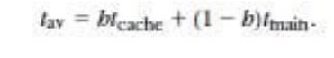
Where tcache is the access time of the cache
and tmain is the main memory access
time. The memory access times are basic parameters available from the memory
manufacturer. The hit rate depends on the program being executed and the cache
organization, and is typically measured using simulators. The best-case memory
access time (ignoring cache controller overhead) is tcache, while the worst-case access time is tmain. Given that tmain
is typically 50– 60 ns for DRAM, while tcache
is at most a few nanoseconds, the spread between worst-case and best-case
memory delays is substantial.
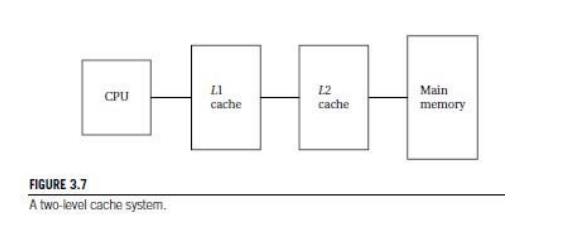
Modern
CPUs may use multiple levels of cache as shown in Figure 3.7. The first-level
cache
(commonly known as L1 cache) is closest to the CPU,
the
second-level cache (L2 cache) feeds the first-level cache, and so on.
The
second-level cache is much larger but is also slower. If h1 is the first-level hit rate and h2 is the rate at which access hit the second-level cache but not
the first-level cache, then the average access time for a two-level cache
system is
As the
program’s working set changes, we expect locations to be removed from the cache
to make way for new locations. When set-associative caches are used; we have to
think about what happens when we throw out a value from the cache to make room
for a new value. We do not have this problem in direct-mapped caches because
every location maps onto a unique block, but in a set-associative cache we must
decide which set will have its block thrown out to make way for the new block.
One possible replacement policy is least recently used (LRU), that is, throw
out the block that has been used farthest in the past. We can add relatively
small amounts of hardware to the cache to keep track of the time since the last
access for each block. Another policy is random replacement, which requires
even less hardware to implement.
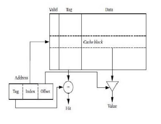
The
simplest way to implement a cache is a direct-mapped cache, as shown in
Figure. The cache consists of cache blocks, each of which includes a tag
to show which memory location is represented by this block, a data field
holding the contents of that memory, and a valid tag to show whether the
contents of this cache block are valid. An address is divided into three
sections. The index is used to select which cache block to check. The tag is
compared against the tag value in the block selected by the index. If the
address tag matches the tag value in the block, that block includes the desired
memory location. If the length of the data field is longer than the minimum
addressable unit, then the lowest bits of the address are used as an offset to
select the required value from the data field. Given the structure of the
cache, there is only one block that must be checked to see whether a location
is in the cache—the index uniquely determines that block. If the access is a
hit, the data value is read from the cache.
Writes
are slightly more complicated than reads because we have to update main memory
as well as the cache. There are several methods by which we can do this. The
simplest scheme is known as write-through—every write changes
both the cache and the corresponding main memory location (usually through a
write buffer).
This
scheme ensures that the cache and main memory are consistent, but may generate
some additional main memory traffic. We can reduce the number of times we write
to main memory by using a write-back policy: If we write only
when we remove a location from the cache, we eliminate the writes when a
location is written several times before it is removed from the cache.
The
direct-mapped cache is both fast and relatively low cost, but it does have
limits in its caching power due to its simple scheme for mapping the cache onto
main memory. Consider a direct-mapped cache with four blocks, in which
locations 0, 1, 2,and 3 all map to different blocks. But locations 4, 8,12,…all
map to the same block as location 0;locations 1, 5, 9,13,…all map to a single
block; and so on. If two popular locations in a program happen to map onto the
same block, we will not gain the full benefits of the cache. As seen in Section
5.6, this can create program performance problems.
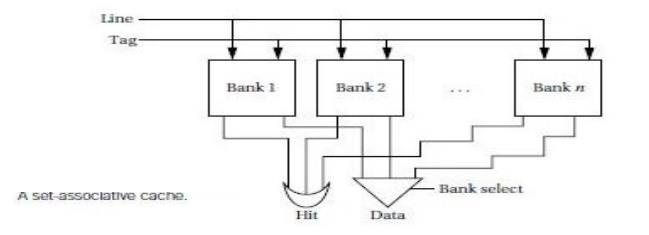
The
limitations of the direct-mapped cache can be reduced by going to the set-associative
cache structure shown in Figure 3.9.A set-associative cache is characterized by
the number of banks or ways it uses, giving an n-way set-associative cache. A set is
formed by all the blocks (one for each bank) that share the
same index. Each set is implemented with a direct-mapped cache. A cache request
is broadcast to all banks simultaneously. If any of the sets has the location,
the cache reports a hit. Although memory locations map onto blocks using the
same function, there are n separate
blocks for each set of locations. Therefore, we can simultaneously Cache
several locations that happen to map onto the same cache block. The set
associative cache structure incurs a little extra overhead and is slightly
slower than a direct-mapped cache, but the higher hit rates that it can provide
often compensate.
The
set-associative cache generally provides higher hit rates than the direct
mapped cache because conflicts between a small numbers of locations can be
resolved within the cache. The set-associative cache is somewhat slower, so the
CPU designer has to be careful that it doesn’t slow down the CPU’s cycle time
too much. A more important problem with set-associative caches for embedded
program design is predictability.
Because
the time penalty for a cache miss is so severe, we often want to make sure that
critical segments of our programs have good behavior in the cache. It is
relatively easy to determine when two memory locations will conflict in a
direct-mapped cache. Conflicts in a set-associative cache are more subtle, and
so the behavior of a set-associative cache is more difficult to analyze for
both humans and programs. Example 3.8 compares the behavior of direct-mapped
and set-associative caches.
Example
Direct-mapped
vs. set-associative caches
For
simplicity, let’s consider a very simple caching scheme. We use 2 bits of the
address as the tag. We compare a direct-mapped cache with four blocks and a
two-way set-associative cache with four sets, and we use LRU replacement to
make it easy to compare the two caches.
A 3-bit
address is used for simplicity. The contents of the memory follow:
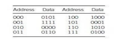
We will
give each cache the same pattern of addresses (in binary to simplify picking
out the index): 001, 010, 011, 100, 101, and 111.
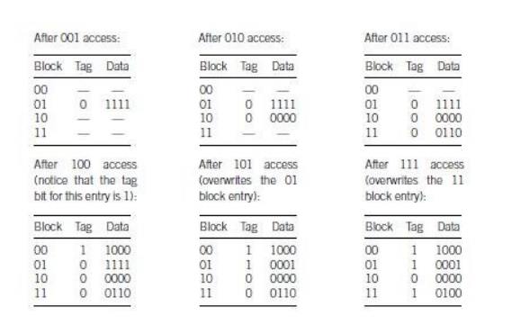
To
understand how the direct-mapped cache works, let’s see how its state evolves.
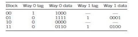
We can
use a similar procedure to determine what ends up in the two-way
set-associative cache. The only difference is that we have some freedom when we
have to replace a block with new data. To make the results easy to understand,
we use a least-recently-used replacement policy. For starters, let’s make each
way the size of the original direct-mapped cache. The final state of the two-way
set-associative cache follows:
Of
course, this is not a fair comparison for performance because the two-way set
associative cache has twice as many entries as the direct-mapped cache. Let’s
use a two-way, set-associative cache with two sets, giving us four blocks, the
same number as in the direct-mapped cache. In this case, the index size is
reduced to 1 bit and the tag grows to 2 bits.
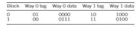
In this
case, the cache contents are significantly different than for either the
direct-mapped cache or the four-block, two-way set-associative cache. The CPU
knows when it is fetching an instruction (the PC is used to calculate the
address, either directly or indirectly) or data. We can therefore choose
whether to cache instructions, data, or both. If cache space is limited,
instructions are the highest priority for caching because they will usually
provide the highest hit rates.
A cache
that holds both instructions and data is called a unified cache.
Various
ARM implementations use different cache sizes and organizations [Fur96]. The
ARM600 includes a 4-KB, 64-way (wow!) unified instruction/data cache.The
StrongARM uses a 16-KB,32-way instruction cache with a 32-byte block and a
16-KB,32-way data cache with a 32-byte block; the data cache uses a write-back
strategy.
The
C5510, one of the models of C55x, uses a 16-K byte instruction cache organized
as a two-way set-associative cache with four 32-bit words per line. The
instruction cache can be disabled by software if desired. It also includes two
RAM sets that are designed to hold large contiguous blocks of code. Each RAM
set can hold up to 4-K bytes of code organized as 256 lines of four 32-bitwords
per line. Each RAM has a tag that specifies what range of addresses is in the
RAM; it also includes a tag valid field to show whether the RAM is in use and
line valid bits for each line.
Memory Management Units and Address Translation
AMMU
translates addresses between the CPU and physical memory. This translation
process is often known as memory mapping since addresses are
mapped from a logical space into a physical space. MMUs in embedded systems
appear primarily in the host processor. It is helpful to understand the basics
of MMUs for embedded systems complex enough to require them.
Many
DSPs, including the C55x, do not use MMUs. Since DSPs are used for
compute-intensive tasks, they often do not require the hardware assist for
logical address spaces. Early computers used MMUs to compensate for limited
address space in their instruction sets. When memory became cheap enough that
physical memory could be larger than the address space defined by the
instructions, MMUs allowed software to manage multiple programs in a single
physical memory, each with its own address space.
Because
modern CPUs typically do not have this limitation, MMUs are used to provide virtual
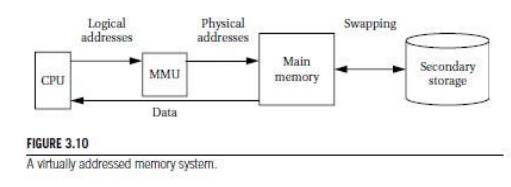
addressing. As shown in Figure 3.10, the MMU accepts logical addresses
from the CPU. Logical addresses refer to the program’s abstract address
space but do not correspond to actual RAM locations. The MMU translates them
from tables to physical addresses that do correspond to RAM. By changing the
MMU’s tables, you can change the physical location at which the program resides
without modifying the program’s code or data. (We must, of course, move the
program in main memory to correspond to the memory mapping change.)
Furthermore,
if we add a secondary storage unit such as flash or a disk, we can eliminate
parts of the program from main memory. In a virtual memory system, the MMU keeps
track of which logical addresses are actually resident in main memory; those
that do not reside in main memory are kept on the secondary storage device.
When the
CPU requests an address that is not in main memory, the MMU generates an
exception called a page fault. The handler for this exception executes code that
reads the requested location from the secondary storage device into main
memory.
The program that generated the page fault is
restarted by the handler only after the required memory has been read back into
main memory, and The MMU’s tables have been updated to reflect the changes.
Of
course, loading a location into main memory will usually require throwing
something out of main memory. The displaced memory is copied into secondary
storage before the requested location is read in. As with caches, LRU is a good
replacement policy.
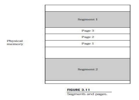
There are
two styles of address translation: segmented and paged. Each has
advantages and the two can be combined to form a segmented, paged addressing
scheme. As illustrated in Figure 3.11, segmenting is designed to support a
large, arbitrarily sized region of memory, while pages describe small, equally
sized regions.
A segment
is usually described by its start address and size, allowing different segments
to be of different sizes. Pages are of uniform size, which simplifies the
hardware required for address translation. A segmented, paged scheme is created
by dividing each segment into pages and using two steps for address
translation.
Paging
introduces the possibility of fragmentation as program pages are
scattered around physical memory.
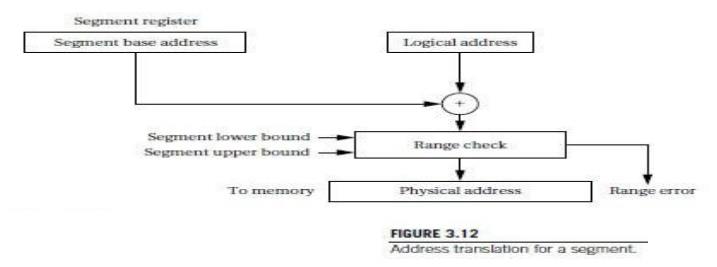
In a
simple segmenting scheme, shown in Figure 3.12,the MMU would maintain a segment
register that describes the currently active segment. This register would point
to the base of the current segment. The address extracted from an instruction
(or from any other source for addresses, such as a register) would be used as
the offset for the address. The physical address is formed by adding the
segment base to the offset. Most segmentation schemes also check the physical
address against the upper limit of the segment by extending the segment
register to include the segment size and comparing the offset to the allowed
size.
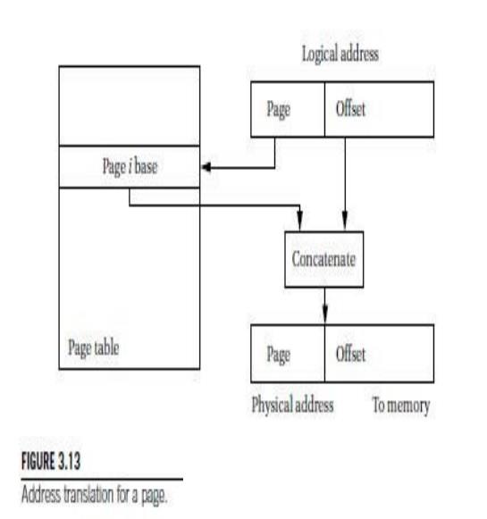
The
translation of paged addresses requires more MMU state but a simpler
calculation. As shown in Figure 3.13, the logical address is divided into two
sections, including a page number and an offset. The page number is used as an
index into a page table, which stores the physical address for the start of
each page. However since all pages have the same size and it is easy to ensure
that page boundaries fall on the proper boundaries, the MMU simply needs to
Concatenate
the top bits of the page starting address with the bottom bits from the page
offset to form the physical address. Pages are small, typically between 512
bytes and 4 KB. As a result, the page table is large for architecture with a
large address space. The page table is normally kept in main memory, which means
that an address translation requires memory access.
The page
table may be organized in several ways, as shown in Figure 3.14. The simplest
scheme is a flat table. The table is indexed by the page number and each entry
holds the page descriptor. A more sophisticated method is a tree. The root
entry of the tree holds pointers to pointer tables at the next level of the
tree; each pointer table is indexed by a part of the page number. We eventually
(after three levels, in this case) arrive at a descriptor table that includes
the page descriptor we are interested in. A tree-structured page table incurs
some overhead for the pointers, but it allows us to build a partially populated
tree. If some part of the address space is not used, we do not need to build
the part of the tree that covers it.
The
efficiency of paged address translation may be increased by caching page
translation information. A cache for address translation is known as a translation
look aside buffer (TLB).The MMU reads the TLB to check
whether a page number is currently in the TLB cache and, if so, uses that
value rather than reading from memory.
Virtual
memory is typically implemented in a paging or segmented, paged scheme so that
only page-sized regions of memory need to be transferred on a page fault. Some
extensions to both segmenting and paging are useful for virtual memory:
■ at
minimum, a present bit is necessary to show
Related Topics