Chapter: Embedded Systems
Important Short Questions and Answers: Embedded Computing
EMBEDDED COMPUTING
1. Define Embedded Systems with examples.
Embedded
system is defined as any device that includes a programmable computer but is
not itself intended to be a general-purpose computer.
Examples:
Mobile Phone, Microwave Oven
2. Write the sequence of design process of an
embedded system.
Requirements,
Specification, Architecture, designing hardware and software components and
integration
3. Differentiate between Microcontroller and Microprocessor.
Microprocessor
is typically designed to be general purpose processor which requires separate
external memory and I/O interfaces. Example:
ARM Processor
Microcontrollers
can be considered as self-contained, cost effective systems with a processor,
on chip memory and Input/Output peripherals built into a single package. Example: 8051 Microcontroller
4. What are functional and non-functional
requirements?
Functional
description gives the basic functions of the embedded system being designed.
Non-functional requirements are the other requirements such as performance,
cost, physical size and weight, power consumption etc.
5. Why system integration phase is difficult?
System
integration is difficult because it usually uncovers problems. It is often hard
to observe the system in sufficient detail to determine exactly what is wrong
because the debugging facilities for embedded systems are usually much more
limited than what you would find on desktop systems.
6. Differentiate between Von-Neumann and Harvard
architecture. Harvard
It
contains Separate memory for both program and data Self Modifying programs are
difficult to write
Von Neumann
It
contains same memory for both program and data More possibility of self
Modifying programs
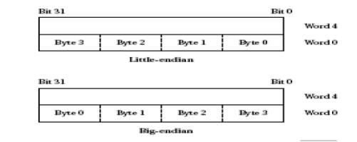
7. Differentiate big and little-endian byte ordering
modes.

8. Give the difference between RISC and CISC
architecture.
CISC
Contains
complex instruction set Contains more addressing modes
RISC
Contains
simple instruction set Contains few addressing modes
9. What is the use of CPSR register?
Current
Program Status Register in ARM is set automatically during every arithmetic,
logical, or shifting operation. The top four bits of the CPSR hold useful
information about the results of that arithmetic/logical operation.
10. Give the details of CSPR register
(N)Negative-The
negative (N) bit is set when the result is negative in two’scomplement
arithmetic.
(Z)
Zero-The zero (Z) bit is set when every bit of the result is zero. (C)Carry-The
carry (C) bit is set when there is a carry out of the operation.
(V)
Overflow- The overflow (V) bit is set when an arithmetic operation results in
an overflow.
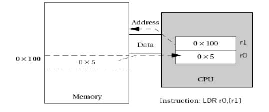
11. Give an example for register indirect
addressing in ARM.

12. What is post indexing addressing mode in ARM?
In
Post-indexing addressing mode the offset is not added to base register until
after the fetch from the base register has been performed.
13. What is base plus offset addressing in ARM.
Base plus
offset addressing does not use register value in base register directly as an
address, the register value is added to another value to form the address. The
added value is called the offset.
14. What are the components of an 8051
microcontroller?
The 8051
microcontroller has 128 bytes of RAM, 4K bytes of on-chip ROM, Two timers, one
serial port, four I/O ports, each 8 bits wide and 6 interrupt sources.
15. Name the most widely used registers in 8051.
The most widely used registers in 8051 are A
(Accumulator) for all arithmetic and logic instructions B, R0, R1, R2, R3, R4,
R5, R6, R7, DPTR (data pointer), and PC (program counter).
16. What is program status word register? Give its
structure.
The
program status word (PSW) register, also referred to as the flag register, is
an 8 bit register. Only 6 bits are used and these four are CY (carry), AC
(auxiliary carry), P (parity), and OV (overflow) are called conditional flags,
meaning that they indicate some conditions that resulted after an instruction
was executed. The PSW3 and PSW4 are designed as RS0 and RS1, and are used to
change the register bank. The two unused bits are user-definable.

17. Give the structure of RAM in 8051.
There are
128 bytes of RAM in the 8051 and the assigned addresses are from 00 to 7FH. The
128 bytes are divided into three different groups as follows:
1) A
total of 32 bytes from locations 00 to 1F hex are set aside for register banks
and the
stack
2) A total
of 16 bytes from locations 20H to 2FH are set aside for bit addressable
read/write memory
3) A total
of 80 bytes from locations 30H to 7FH are used for read and write storage,
called scratch pad.
18.
How can
you switch to other register banks in 8051 microcontroller?
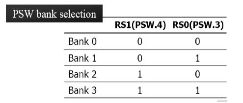
We can
switch to other banks by use of the PSW register. Bits D4 and D3 of the PSW are
used to select the desired register bank. We use the bit-addressable
instructions SETB and CLR to access PSW.4 and PSW.3.

19. What is the default register bank in 8051?
RAM
locations from 0 to 7 are set aside for bank 0 of R0-R7 where R0 is RAM
location 0. Register bank 0 is the default when 8051 is powered up.
20. How are stacks accessed in 8051?
The
register used to access the stack is called the SP (stack pointer) register.
The stack pointer register is only 8 bits wide and can take values of 00 to
FFH. When 8051 is powered up, the SP contains value 07. This means RAM location
08 is the first location being used for the stack by 8051.
21.
Name some
of the hardware parts of embedded systems?
Power source
Clock oscillator circuit
Timers
Memory units
DAC and ADC
LCD and LED displays
Keyboard/Keypad
Related Topics