Chapter: 11th 12th std standard Class Physics sciense Higher secondary school College Notes
Extrinsic semiconductor: N and P -type semiconductor

Extrinsic semiconductor
An extrinsic semiconductor is one
in which an impurity with a valency higher or lower than the valency of the
pure semiconductor is added, so as to increase the electrical conductivity of
the semiconductor.
Depending upon the type of
impurity atoms added, an extrinsic semiconductor can be classified as N-type or
P-type.
(a) N-type semiconductor
When a small amount of
pentavalent impurity such as arsenic is added to a pure germanium semiconductor
crystal, the resulting crystal is called N-type semiconductor.

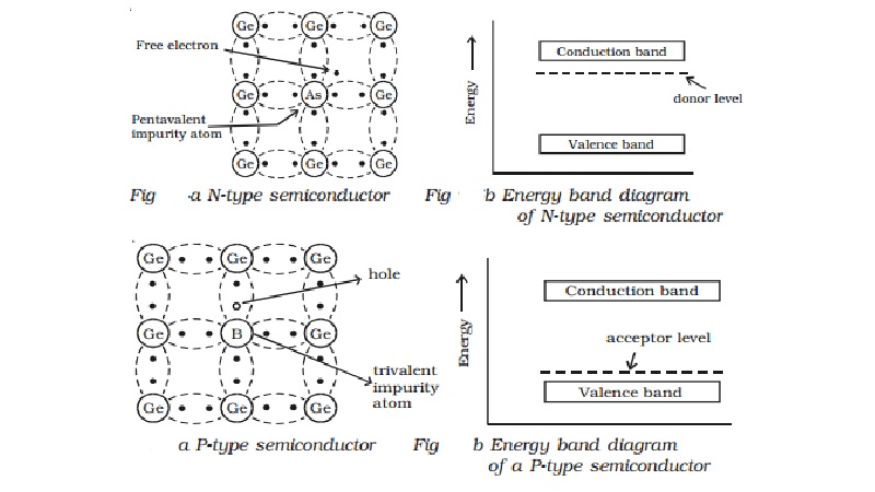
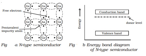
Fig a shows the crystal structure
obtained when pentavalent arsenic impurity is added with pure germanium
crystal. The four valence electrons of arsenic atom form covalent bonds with
electrons of neighbouring four germanium atoms. The fifth electron of arsenic
atom is loosely bound. This electron can move about almost as freely as an
electron in a conductor and hence it will be the carrier of current. In the
energy band picture, the energy state corresponding to the fifth valence
electron is in the forbidden gap and lies slightly below the conduction band
(Figb). This level is known as the donor level.
When the fifth valence electron
is transferred to the conduction band, the arsenic atom becomes positively
charged immobile ion. Each impurity atom donates one free electron to the
semiconductor. These impurity atoms are called donors.
In N-type semiconductor material,
the number of electrons increases, compared to the available number of charge
carriers in the intrinsic semiconductor. This is because, the available larger
number of electrons increases the rate of recombination of electrons with
holes. Hence, in N-type semiconductor, free electrons are the majority charge
carriers and holes are the minority charge carriers.
(b) P-type semiconductor
When a small amount of trivalent
impurity (such as indium, boron or gallium) is added to a pure semiconductor
crystal, the resulting semiconductor crystal is called P-type semiconductor.

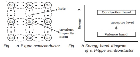
Fig a. shows the crystal
structure obtained, when trivalent boron impurity is added with pure germanium
crystal. The three valence electrons of the boron atom form covalent bonds with
valence electrons of three neighbourhood germanium atoms. In the fourth
covalent bond, only one valence electron is available from germanium atom and
there is deficiency of one electron which is called as a hole. Hence for each
boron atom added, one hole is created. Since the holes can accept electrons
from neighbourhood, the impurity is called acceptor. The hole, may be filled by
the electron from a neighbouring atom, creating a hole in that position from
where the electron moves. This process continues and the hole moves about in a
random manner due to thermal effects. Since the hole is associated with a
positive charge moving from one position to another, this is called as P-type
semiconductor. In the P-type semiconductor, the acceptor impurity produces an
energy level just above the valence band. (Fig b). Since, the energy difference
between acceptor energy level and the valence band is much smaller, electrons
from the valence band can easily jump into the acceptor level by thermal
agitation.
In P-type semiconductors, holes
are the majority charge carriers and free electrons are the minority charge
carriers.
Related Topics