Chapter: 11th 12th std standard Class Physics sciense Higher secondary school College Notes
PN Junction diode: Forward and Reverse bias characteristics
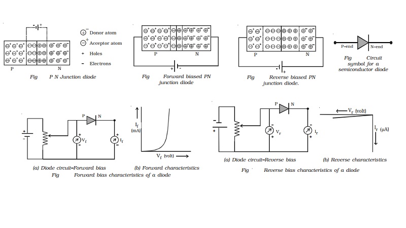
PN Junction diode
If one side of a single crystal
of pure semiconductor (Ge or Si) is doped with acceptor impurity atoms and the
other side is doped with donor impurity atoms, a PN junction is formed as shown
in Fig. P region has a high concentration of holes and N region contains a
large number of electrons.
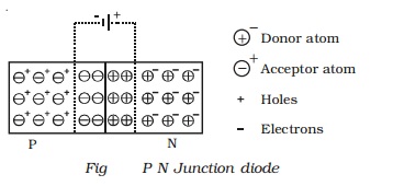
As soon as the junction is
formed, free electrons and holes cross through the junction by the process of
diffusion. During this process, the electrons crossing the junction from
N-region into the P region, recombine with holes in the P-region very close to
the junction. Similarly holes crossing the junction from the P-region into the
N-region, recombine with electrons in the N-region very close to the junction.
Thus a region is formed, which does not have any mobile charges very close to the
junction. This region is called depletion region. In this region, on the left
side of the junction, the acceptor atoms become negative ions and on the right
side of the junction, the donor atoms become positive ions (Fig).
An electric field is set up, between
the donor and acceptor ions in the depletion region. The potential at the
N-side is higher than the potential at P-side. Therefore electrons in the
N-side are prevented to go to the lower potential of P-side. Similarly, holes
in the P-side find themselves at a lower potential and are prevented to cross
to the N-side. Thus, there is a barrier at the junction which opposes the
movement of the majority charge carriers. The difference of potential from one
side of the barrier to the other side is called potential barrier. The
potential barrier is approximately 0.7V for a silicon PN junction and 0.3V for
a germanium PN junction. The distance from one side of the barrier to the other
side is called the width of the barrier, which depends upon the nature of the
material.
Forward biased PN junction diode
When the positive terminal of the
battery is connected to P-side and negative terminal to the N-side, so that the
potential difference acts in opposite direction to the barrier potential, then
the PN junction diode is said to be forward biased.
When the PN junction is forward
biased (Fig), the applied positive
potential repels the holes in the P-region, and the applied negative potential
repels the electrons in the N-region, so the charges move towards the junction.
If the applied potential difference is more than the potential barrier, some
holes and free electrons enter the depletion region.
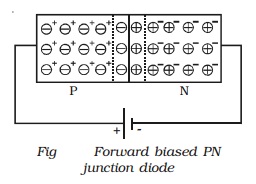
Hence, the potential barrier as
well as the width of the depletion region are reduced. The positive donor ions
and negative acceptor ions within the depletion region regain electrons and
holes respectively. As a result of this, the depletion region disappears and
the potential barrier also disappears. Hence, under the action of the forward
potential difference, the majority charge carriers flow across the junction in
opposite direction and constitute current flow in the forward direction.
Reverse biased PN junction diode
When the positive terminal of the
battery is connected to the N-side and negative terminal to the P-side, so that
the applied potential difference is in the same direction as that of barrier
potential, the junction is said to be reverse biased.
When the PN junction is reverse
biased (Fig), electrons in the N region and holes in the P-region are attracted
away from the junction.
Because of this, the number of
negative ions in the P-region and positive ions in the N-region increases.
Hence the depletion region becomes wider and the potential barrier is
increased.
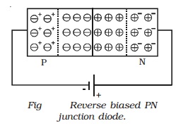
Since the depletion region does
not contain majority charge carriers, it acts like an insulator. Therefore, no
current should flow in the external circuit. But, in practice, a very small
current of the order of few microamperes flows in the reverse direction. This
is due to the minority carriers flowing in the opposite direction. This reverse
current is small, because the number of minority carriers in both regions is
very small. Since the major source of minority carriers is, thermally broken
covalent bonds, the reverse current mainly depends on the junction temperature.
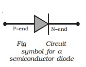
Symbol for a semiconductor diode
The diode symbol is shown in Fig.
The P-type and N-type regions are referred to as P-end and N-end respectively.
The arrow on the diode points the direction of conventional current.
Forward bias characteristics
The circuit for the study of
forward bias characteristics of PN junction diode is shown in Fig a. The
voltage between P-end and N-end is increased from zero in suitable equal steps
and the corresponding currents are noted down. Fig b shows the forward bias
characteristic curve of the diode. Voltage is the independent variable.
Therefore, it is plotted along X-axis. Since, current is the dependent
variable, it is plotted against Y-axis. From the
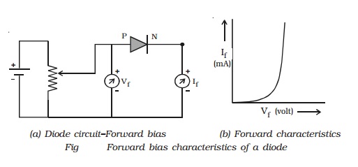
characteristic curve, the following conclusions can be made. (i)
The forward characteristic is not a straight line. Hence the ratio V/I is not a
constant (i.e) the diode does not obey Ohm's law. This implies that the
semiconductor diode is a non-linear conductor of electricity. (ii) It can be
seen from the characteristic curve that initially, the current is very small.
This is because, the diode will start conducting, only when the external
voltage overcomes the barrier potential (0.7V for silicon diode). As the
voltage is increased to 0.7 V, large number of free electrons and holes start
crossing the junction. Above 0.7V, the current increases rapidly. The voltage
at which the current starts to increase rapidly is known as cut-in voltage or
knee voltage of the diode.
Reverse bias characteristics
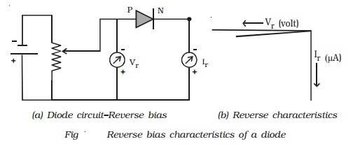
The circuit for the study of
reverse bias characteristics of PN junction diode is shown in Fig a. The
voltage is increased from zero in suitable steps. For each voltage, the
corresponding current readings are noted down. Fig b shows the reverse bias
characteristic curve of the diode. From the characteristic curve, it can be
concluded that, as voltage is increased from zero, reverse current (in the
order of microamperes) increases and reaches the maximum value at a small value
of the reverse voltage. When the voltage is further increased, the current is
almost independent of the reverse voltage upto a certain critical value. This
reverse current is known as the reverse saturation current or leakage current.
This current is due to the minority charge carriers, which depends on junction
temperature.
Related Topics