Chapter: Embedded Systems
8051 Microcontroller
EMBEDDED PROCESSORS
Embedded
processors can be broken into two broad categories: ordinary microprocessors
(μP) and microcontrollers (μC), which have many more peripherals on chip,
reducing cost and size.
Contrasting
to the personal computer and server markets, a fairly large number of basic CPU
architectures are used; there are Von Neumann as well as various degrees of
Harvard architectures, RISC as well as non-RISC and VLIW; word lengths vary
from 4-bit to 64-bits and beyond (mainly in DSP processors) although the most
typical remain 8/16-bit. Most architecture comes in a large number of different
variants and shapes, many of which are also manufactured by several different
companies. e.g ARM
8051 MICROCONTROLLER
8051 is
an excellent device for building many embedded systems. One important factor is
that the 8051 requires a minimum number of external components in order to
operate.
It is a
well-tested design; introduced in its original form by Intel in 1980 the
development costs of this device now start at less than US $1.00. At this
price, you get a performance of around 1 million instructions per second, and
256 bytes (not megabytes!) of
on-chip RAM, 32 port pins and a serial interface.
Features of 8051:
The main features of 8051 microcontroller are:
RAM – 128
Bytes (Data memory) ROM – 4Kbytes .
Serial
Port – Using UART makes it simpler to interface for serial communication.
Two 16
bit Timer/ Counter, Input/output Pins – 4 Ports of 8 bits each on a single
chip. 6 Interrupt Sources
8 – bit
ALU (Arithmetic Logic Unit)
Harvard
Memory Architecture – It has 16 bit Address bus (each of RAM and ROM) and 8 bit
Data Bus.
8051 can
execute 1 million one-cycle instructions per second with a clock frequency of
12MHz.
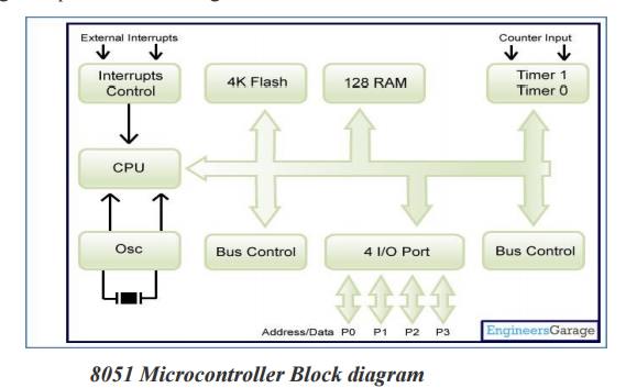
This microcontroller is also called as “System on a chip”
because it has all the features on
a single chip. The Block Diagram of 8051 Microcontroller is as
shown in Figure
Pin
configuration of 8051
The
following is the Pin diagram of 8051 microcontroller.
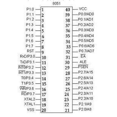
A) BASIC PINS
PIN 9: PIN 9 is the reset pin which is
used to reset the microcontroller’s internal registers and ports upon starting up. (Pin should be held high for 2 machine
cycles.)
PINS 18 & 19: The 8051 has a built-in
oscillator amplifier hence we need to only connect a crystal at these pins to provide clock pulses
to the circuit.
PIN 40 and 20: Pins 40 and 20 are VCC and
ground respectively. The 8051 chip needs +5V 500mA to function properly, although there are lower powered
versions like the Atmel 2051 which is a scaled down version of the 8051 which
runs on +3V.
PINS 29, 30 & 31: As
described in the features of the 8051, this chip contains a built-in flash memory. In order to program this we
need to supply a voltage of +12V at pin 31. If external memory is connected
then PIN 31, also called EA/VPP, should be connected to ground to indicate the
presence of external memory. PIN 30 is called ALE (address latch enable), which
is used when multiple memory chips are connected to the controller and only one
of them needs to be selected. PIN 29 is called PSEN. This is "program
store enable". In order to use the external memory it is required to
provide the low voltage (0) on both PSEN and EA pins.
B) PORTS
There are
4 8-bit ports: P0, P1, P2 and P3.
PORT P1 (Pins 1 to 8): The
port P1 is a general purpose input/output port which can be used for a variety of interfacing tasks. The
other ports P0, P2 and P3 have dual roles or additional functions associated
with them based upon the context of their usage.
PORT P3 (Pins 10 to 17): PORT P3
acts as a normal IO port, but Port P3 has additional functions such as, serial transmit and receive
pins, 2 external interrupt pins, 2 external counter inputs, read and write pins
for memory access.
PORT P2 (pins 21 to 28): PORT P2
can also be used as a general purpose 8 bit port when no external memory is present, but if external memory access is
required then PORT P2 will act as an address bus in conjunction with PORT P0 to
access external memory. PORT P2 acts as A8-A15, as can be seen from fig 1.1
PORT P0 (pins 32 to 39) PORT P0
can be used as a general purpose 8 bit port when no external emory is present, but if external memory
access is required then PORT P0 acts as multiplexed address and data bus that
can be used to access external memory in conjunction with PORT P2. P0 acts as
AD0-AD7.
C) OSCILLATOR CIRCUITS
The 8051
requires the existence of an external oscillator circuit. The oscillator
circuit usually runs around 12MHz, although the 8051 (depending on which
specific model) is capable of running at a maximum of 40MHz. Each machine cycle
in the 8051 is 12 clock cycles, giving an effective cycle rate at 1MHz (for a
12MHz clock) to 3.33MHz (for the maximum 40MHz clock). The oscillator circuit
generates the clock pulses so that all internal operations are synchronized.
The
external interface of the Standard 8051
Small 8051
Low-cost
members of the 8051 family with reduced number of port pins, and no support for
off-chip memory. Typical application:
Low-cost consumer goods.
Standard 8051: The Small 8051s and the Extended
8051s are derived
Extended 8051:Members of the 8051 family with
extended range of no-chip facilities (e.g.
CAN controllers, ADC, DAC,etc), large numbers of port pins, and - in recent
devices - support for large amounts of off-chip memory. Typical applications: Industrial and automotive systems.
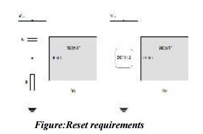
Reset
requirements
‘Reset
routine’ must be run to place hardware into an appropriate state before it can
begin executing the user program. Running this reset routine takes time, and
requires that the microcontroller’s oscillator is operating.
Where
system is supplied by a robust power supply, which rapidly reaches its
specified output voltage when switched on, rapidly decreases to 0V when
switched off, and – while switched on – cannot ‘brown out’ (drop in voltage),
then we can safely use low-cost reset hardware based on a capacitor and a
resistor to ensure that system will be reset correctly: this form of reset
circuit is shown in Figure
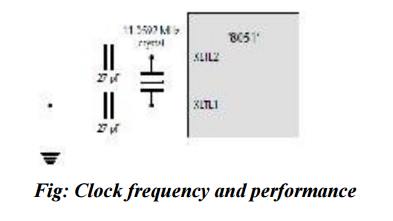
Clock
frequency and performance
All
digital computer systems are driven by some form of oscillator circuit: the
8051 is certainly no exception. If the oscillator fails, the system will not
function at all; if the oscillator runs irregularly, any timing calculations
performed by the system will be inaccurate.
Memory
Issues
A. Types of memory
Dynamic RAM (DRAM)
Static RAM (SRAM)
Mask Read-Only Memory (ROM)
Programmable Read-Only Memory (PROM)
UV
Erasable Programmable Read-Only Memory (UV EPROM)
EEPROM
and Flash ROM
v Dynamic
RAM Vs Static RAM
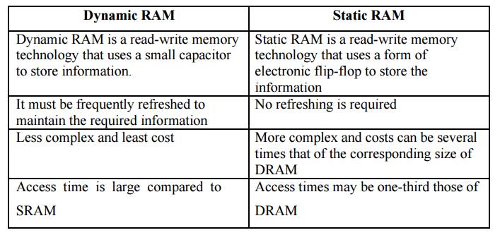
Dynamic RAM
Dynamic
RAM is a read-write memory technology that uses a small capacitor to store
information.
It must
be frequently refreshed to maintain the required information Less complex and
least cost
Access
time is large compared to SRAM
Static RAM
Static
RAM is a read-write memory technology that uses a form of electronic flip-flop
to store the information
No
refreshing is required
More
complex and costs can be several times that of the corresponding size of DRAM
Access
times may be one-third those of DRAM
v Mask
Read-Only Memory (ROM):
Mask ROM
is – from the software developer’s perspective – read only; A ‘mask’ is
provided by the company for which the chips are being produced. Such devices
are therefore sometimes referred to as ‘factory programmed”.
v Programmable
Read-Only Memory (PROM)
PROM is a
form of Write-Once, Read-Many (WORM) or ‘One-Time Programmable’ (OTP) memory.
Basically, we use a PROM programmer to blow tiny ‘fuses’ in the device.
v UV
Erasable Programmable Read-Only Memory (UV EPROM) :
UV EPROMs are programmed electrically. Unlike
PROMs, they also have a quartz window which allows the memory to be erased by
exposing the internals of the device to UV light.
v EEPROM
and Flash ROM
Electrically-Erasable
Programmable Read-Only Memory (EEPROMs) and ‘Flash’ ROMs are a more
user-friendly form of ROM that can be both programmed and erased electrically.
EEPROM and Flash ROM are very similar. EEPROMs can usually be reprogrammed on a
byte-by-byte basis, and are often used to store passwords or other ‘persistent’
user data. Flash ROMs generally require a block-sized ‘erase’ operation before
they can be programmed.
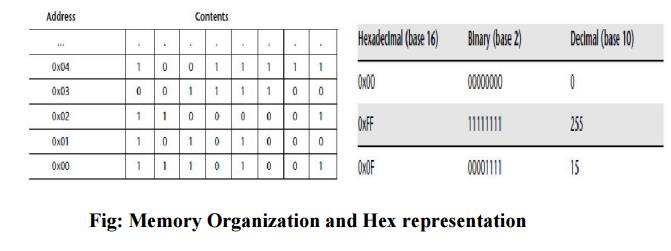
b) Memory
organization and ‘hex’
All data
items are represented in computer memory as binary codes, each containing a
certain number of bits. To simplify the storage and retrieval of data items,
these memory bits are organized into memory locations, each with a unique
memory address. The other Memory representations are shown
C) The 8051 memory architecture
There are
two distinct memory regions in an 8051 device: the DATA area and the CODE area.
DATA
memory : DATA memory is used to store variables and the program stack while the
program is running. The DATA area will be implemented using some form of RAM.
Most of the DATA area has a byte-oriented memory organization. However, within
the DATA area is a 16-byte BDATA area which can also be accessed using bit
addresses.
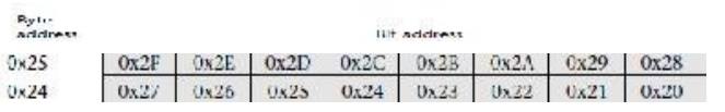
The
compiler avoids confusion if 0x24 in bit address and byte address.
ü CODE memory :CODE area is used to store the
program code, usually in some form of ROM.
The CODE area may also contain read-only variables (‘constants’), such as
filter co-efficients or data for speech playback.
D) 8-bit
family, 16-bit address space
An ‘8-bit
microcontroller’ refers to the size of the registers and data bus. This means
that the family will handle 8-bit data very quickly and process 16-bit or
32-bit data rather less efficiently. The 16-bit address space means that the
device can directly address 216 bytes of memory: that is, 64 kbytes.
E) I/O
pins
Most
8051s have four 8-bit ports, giving a total of 32 pins you can individually
read from or control. All of the ports are bidirectional: that is, they may be
used for both input and output
F) Timers
All
members of the 8051 family have at least two timer/counters, known as Timer 0
and Timer 1: most also have an additional timer (Timer 2). These are 16-bit
timers, they can hold values from 0 to 65535 (decimal).There are many things we
can do with such a timer:
It
used to measure intervals of time. It can measure the duration of a function by
noting the value of a timer at the beginning and end of the function call, and
comparing the two
results.
Use
it to generate precise hardware delays.
Use it to
generate ‘time out’ facilities: this is a key requirement in systems with
real-time constraints.
Most important of all, we can use it to generate regular ‘ticks’, and drive
an operating system
G.
Interrupts
An
interrupt is a hardware mechanism used to notify a processor that an ‘event’
has taken place: such events may be ‘internal’ events (such as the overflow of
a timer) or ‘external’ events
(such as
the arrival of a character through a serial interface).The original ‘8051’
(‘8052’) architecture supported seven interrupt sources:
·
Two or three timer/counter interrupts
·
Two UART-related
·
Two external interrupts
The
‘power-on reset’ (POR) interrupt. In Figure the system executes two
(background) functions, Function 1 and Function 2 . During the execution of
Function 1, an interrupt is raised, and an ‘interrupt service routine’ (ISR1)
deals with this event. After the execution of ISR1 is complete, Function 1
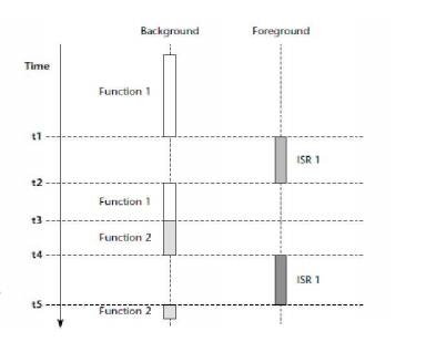
another
interrupt is raised, this time dealt with by ISR 2.
H. Serial
interface
Such an
interface is common in embedded processors, and is widely used. Here are some
examples:
The
serial port may be used to debug embedded applications, using a desktop PC.
The
serial port may be used to load code into flash memory for ‘in circuit
programming’
The
serial port may be used to transfer data from embedded data acquisition systems
to a PC, or to other embedded processors
I .Power
consumption
All modern
implementations of 8051 processors have at least three operating modes:
Normal
mode. Idle Mode.
Power-Down
Mode.
The
‘Idle’ and ‘Power Down’ modes are intended to be used to save power at times
when no processing is required .We generally aim for an average power
consumption of less than 10 mA.
Idle
mode: In the idle mode the oscillator of the C501 continues to run, but the CPU
is gated off from the clock signal. Rhe
interrupt system, the serial port and all timers are connected to the clock.
The idle mode is entered by setting the flag bit IDLE (PCON.0). The easiest
way is:
PCON |= 0x01; // Enter idle mode
There are
two ways as activating any enabled interrupt and Perform a hardware reset.
ü
Power-down mode:
The
power-down mode is entered by setting the flag bit PDE (PCON.1). This is done
in ‘C’ as follows:
PCON |= 0x02; // Enter power-down
mode
The only
exit from power-down mode is a hardware reset.
Related Topics