Chapter: 11th 12th std standard Class Physics sciense Higher secondary school College Notes
Working of a PNP transistor
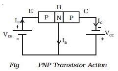
Working of a PNP transistor
A PNP transistor is like two PN junction
diodes, which are placed back-to-back. At each junction, there is a depletion
region which gives rise to a potential barrier. The external biasing of the
junction is provided by the batteries VEE and VCC as shown in Fig.. The emitter
base junction is forward biased and the collector base junction is reverse
biased.

Since the emitter-base junction is forward
biased, a large number of holes cross the junction and enters the base. At the
same time, very few electrons flow from the base to the emitter. These
electrons, when they reach emitter, recombine with an equal number of holes in
the emitter. The loss of total number of holes in the emitter is made by flow
of an equal number of electrons from the emitter to the positive terminal of
the battery. The flow of holes from the emitter to base gives rise to emitter
current IE. In the emitter, IE is due to the flow of
holes. But in the external circuit the current is due to the flow of electrons
from the emitter to the positive terminal of the battery VEE. The
holes diffuse through the base. These holes take a very small time to flow
through this region before they reach the depletion region. During this time, a
very small number of holes recombine with an equal number of electrons in the
base. Because the base is lightly doped and very thin, this number is very
small. The loss of total number of electrons per second is made up by the flow
of an equal number of electrons from the negative terminal of VEE
into the base. The flow of these electrons contribute the base current IB.
The remaining numbers of holes, which do not
undergo recombination process in the base, reach the collector. These are
neutralised by an equal number of electrons flowing from the negative terminal
of the battery VCC into the collector. At the same time, an equal
number of electrons flows from the negative terminal of VEE and
reach the positive terminal of VCC. The flow of holes per second
from the base to the collector gives rise to the collector current Ic
from the base to the collector. In the external circuit, it is due to the flow
of electrons from the negative terminal of the battery VCC into the
collector.
Applying Kirchoff's current law to the circuit,
the emitter current is the sum of collector current and base current.
i.e IE
= IB + IC
This equation is the fundamental
relation between the currents in a transistor circuit.
This equation is true regardless
of transistor type or transistor configuration.
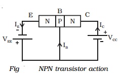
The action of NPN transistor
(Fig) is similar to that of PNP transistor.
Related Topics