Chapter: 11th 12th std standard Class Physics sciense Higher secondary school College Notes
Transistor circuit configurations
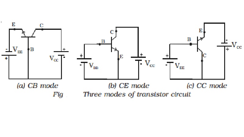
Transistor circuit configurations
There are three types of circuit
connections (called configurations or modes) for operating a transistor. They
are (i) common base (CB) mode (ii) common emitter (CE) mode and (iii) common
collector (CC) mode.
The term common is used to denote
the lead that is common to the input and output circuits. The different modes
are shown in Fig for NPN transistor.
In a similar way, three
configurations can be drawn for PNP transistor.
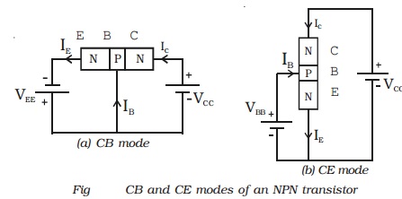
Current amplification factors α and β and the relation between them
The current amplification factor
or current gain of a transistor is the ratio of output current to the input
current. If the transistor is connected in common base mode, the current gain α = IC / IE and if the transistor is
connected in common emitter mode, the current gain β = IC /IB Fig shows a NPN transistor connected in the
common base and common emitter configurations. Since, 95%
of the injected
electrons reach the collector, the collector current is almost equal to the
emitter current. Almost all transistors have � , in the range 0.95 to 0.99.
We know that
α = IC
/IE =IC /(IB+IC)
1/ α = (IB+IC)
/ IC
( 1/ α ) - 1 =
1/ β
β = α / (1- α)
Usually β lies between 50 and 300. Some transistors have β as high as 1000.
Characteristics of an NPN
transistor in common emitter configuration
The three important
characteristics of a transistor in any mode are (i) input characteristics (ii)
output characteristics and (iii) transfer characterstics.
The circuit to study the characteristic curves of NPN transistor
in common emitter mode is as shown in Fig.
(i) Input characteristics
Input characteristic curve is drawn between the base current (IB)
and voltage between base and emitter (VBE), when the voltage between
collector and emitter (VCE) is kept constant at a particular value.
VBE is increased in suitable equal steps and corresponding base
current is noted. The procedure is repeated for different values of VCE.
IB values are plotted against VBE for
constant VCE. The input characteristic thus obtained is shown in
Fig.The input impedance of the transistor is defined as the ratio of small
change in base - emitter voltage to the corresponding change in base current at
a given VCE.
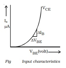
The input impedance of the transistor is defined as the ratio of
small change in base - emitter voltage to the corresponding change in base
current at a given VCE.
∴ Input impedance, r1
= (∆VBE/∆IB)VCE
The input impedance of the transistor in CE mode is very high.
(ii) Output characteristics
Output characteristic curves are
drawn between IC and VCE, when IB is kept
constant at a particular value.
The base current IB is kept at a constant value, by
adjusting the base emitter voltage VBE. VCE is increased
in suitable equal steps and the corresponding collector current is noted. The
procedure is repeated for different values of IB. Now, Ic
versus VCE curves are drawn for different values of IB.
The output characteristics thus obtained are represented in Fig. The three
regions of the characteristics can be discussed as follows :
Saturation region : The initial part of the curve (ohmic region,
OA) is called saturation region. (i.e) The region in between the origin and
knee point. (Knee point is the point, where Ic is about to become a constant).
Cut off region : There is very small collector current in the
transistor, even when the base current is zero (IB = 0). In the
output characteristics, the region below the curve for IB = 0 is
called cut off region. Below the cut off region, the transistor does not function.
Active region : The central region of the curves
is called active region. In the
active region, the curves are uniform. In this region, E-B junction is forward
biased and C-B junction is reverse biased.
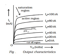
The output impedance ro is defined as the ratio of
variation in the collector emitter voltage to the corresponding variation in
the collector current at a constant base current in the active region of the
transistor characteristic curves.
output impedence, ro = (∆VCE/ ∆IC)IB
The output impedance of a transistor in CE mode is low.
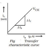
(iii) Transfer characteristics
The transfer characteric curve is drawn between IC and IB, when
VCE is kept constant at a particular value. The base current IB is increased in
suitable steps and the collector current IC is noted down for each value of IB.
The transfer characteristic curve is shown in Fig.
The current gain is defined as the ratio of a small change in
the collector current to the corresponding change in the base current at a
constant VCE.
Current gain, β = (∆IC/ ∆IB)VcE
The common emitter configuration has high input impedance, low
output impedance and higher current gain when compared with common base
configuration.
Related Topics