Chapter: 11th 12th std standard Class Physics sciense Higher secondary school College Notes
Transistor biasing - Voltage divider bias

Transistor biasing
In order to amplify the input
signal using a transistor, the signal is to be applied at an operating point
called Q point in the active region. Once the operating point is established,
its position should not change. If the Q point shifts near the saturation line
or near cut off region of the output characteristics, the signal will be
distorted after amplification.
The proper selection of operating
point of a transistor and maintenance of proper emitter voltage during the
passage of the signal is known as transistor biasing.
The most commonly used methods of
obtaining transistor biasing are (i) base bias, (ii) base bias with emitter feedback,
(iii) base bias with collector feedback and (iv) voltage divider bias.
The principle involved in all
these types is to obtain the required base current corresponding to the
operating point under zero signal conditions.
In all the bias circuits except
voltage divider bias, the collector current depends on the current gain (β) of the transistor. But β of a transistor is very sensitive to temperature
changes. For this reason, it is desirable to have a bias circuit whose action
is independent of β. The requirement is met by the
voltage divider bias circuit.
Voltage divider bias
This is the most widely used
method of providing bias and stabilization to a transisitor. In this method,
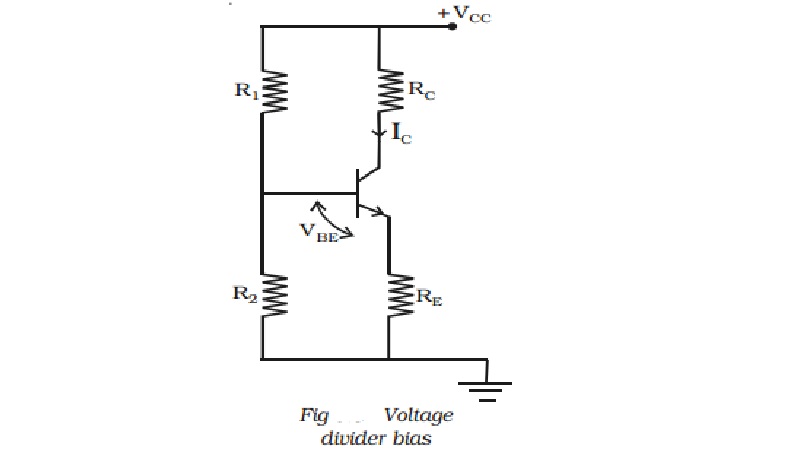
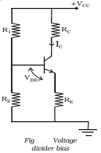
two resistances R1 and R2 are connected across the supply
voltage VCC (Fig) and provide biasing. The emitter resistance RE
provides stabilization. The voltage drop across R2 forward biases
the base emitter junction. This causes the base current and hence collector
current to flow in zero signal conditions.

The stabilization provided by RE
can be explained as follows. Since β is very sensitive to temperature changes,
![]()
![]() the collector current IC increases with
rise in temperature. Consequently, it can be seen that IE increases.
This will cause the voltage drop across emitter resistance RE to
increase. The voltage drop across R2 = VBE + VRE.
As voltage drop across R2 is independent of IC, VBE
decreases. This decreases IB and the reduced value of IB
tends to bring back IC to the original value. Hence any variation of
β will have no effect on the operating point.
the collector current IC increases with
rise in temperature. Consequently, it can be seen that IE increases.
This will cause the voltage drop across emitter resistance RE to
increase. The voltage drop across R2 = VBE + VRE.
As voltage drop across R2 is independent of IC, VBE
decreases. This decreases IB and the reduced value of IB
tends to bring back IC to the original value. Hence any variation of
β will have no effect on the operating point.
Related Topics