Chapter: Embedded Systems Design : Memory systems
The MC68040 burst interface
The MC68040 burst interface
Earlier , some of the problems faced by a designer using
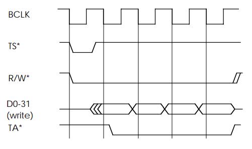
SRAM with a burst interface were discussed. The MC68040 burst interface shows
how these conflicts arise and their solution. It operates on a 2-1-1-1 basis,
where two clock periods are allocated for the first access, and the remaining
accesses are performed each in a single cycle. The first function the interface
must perform is to generate the toggled A2 and A3 addresses from the first
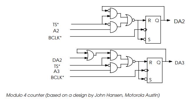
address put out by the MC68040. This involves creating a modulo 4 counter where
the addresses will increment and wrap around. The MC68040 uses the burst access
to fetch four long words for the internal cache line. It will start anywhere in
the line so that the first data that is accessed can be passed to the processor
while the rest of the data is fetched in parallel. This improves performance by
fetching the immediate data first, but it does complicate the address
generation logic — a standard 2 bit counter is not applicable. A typical
circuit is shown.
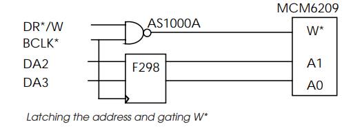
Given the generated addresses, the hardest task for the interface is to
create the write pulse needed to write data to the FSRAMs. The first hurdle is
to ensure that the write pulse com-mences after the addresses have been
generated. The easiest way of doing this is to use the two phases of the BCLK*
to divide the timing into two halves. During the first part, the address is
latched by the rising edge of BCLK*.
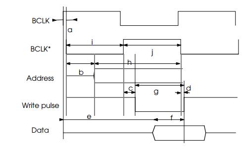
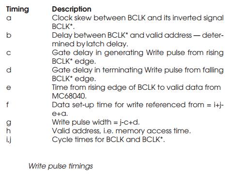
Latching DA2 and DA3 holds the address valid while allowing the modulo 4
counter to propagate the next value through. The falling edge of BCLK* is then
used to gate the read/write signal to create a write pulse. The write pulse is
removed before the next address is latched. This guarantees that the write
pulse will be generated after the address has become valid. This circuit neatly
solves the competing criteria of bringing the write pulse high before the
address can be changed and the need to change the address as early as possible
The table shows the timing and the values for the write
pulse, tWLWH, write data set-up time, tDVWH and the overall access time tAVAV. For both 25 and 33 MHz speeds, the access time is always greater than
20 ns and therefore 20 ns FSRAM would be sufficient.
The difficulty comes in meeting the write pulse and data set-up times. At 25
MHz, the maximum write pulse is 17 ns and the data set-up is 9 ns. Many 20 ns
FSRAMs specify the minimum write pulse width with the same value as the overall
access time. As a result 20 ns access time parts would not meet this
specifica-tion. The data set-up is also longer and it is likely that 15 ns or
faster parts would have to be used. At 33 MHz, the problem is worse.
Related Topics