Chapter: Embedded Systems Design : Memory systems
Memory protection units
Memory protection units
There has been a trend in recent processor designs to include a tripped
down memory management unit that allows the memory to be partitioned and
protected without any address translation. This removes the time consuming
address translation mechanism which reduces the memory access time and the
amount of hardware needed when compared with a full MMU implemen-tation. In
addition with system on a chip designs, this can reduce the chip size, cost and
power consumption although it is fair to say that the size of these units are
small compared to that of the whole chip and especially any on-chip memory. It
is also possible to use the MMU as a memory protection unit by disabling the
address translation or by arranging for the translation to be non-existent i.e.
the physical and logical addresses are the same.
The basic idea behind a memory protection unit is to police the memory
subsystem so that only approved memory accesses can take place. If a memory
access is made to a protected area by software that does not have the correct
access rights, an error signal is generated which can be used to start
supervisor level software to decide what to do.

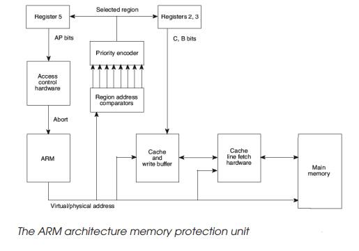
The ARM architecture memory protection unit performs this function. It
can divide the memory range into eight separate regions. Each region can be as
small as 4 kbytes up to 4 Gbyte and its starting address must be on a region
boundary. If region is set to 4 Kbytes then it can start on an address like
0x45431000 but an 8 kbyte region cannot. Its nearest valid address would be
0x45430000 or 0x45432000. Each region has an associated cacheable bit, a
bufferable bit and access permission bits. These control whether the data
stored in the region is cacheable (C bit), can be buffered in the processor's
write buffer (B bit) and the type of access permitted (AP bits). These are in
fact very similar to the permission bits used in the corresponding ARM MMU
architec-ture and are stored in control registers. The regions are numbered and
this defines a priority level for resolving which permission bits take
precedence if regions overlap. For example region 2 may not permit data caching
while region 6 does. If region 6 overlaps region 2, then the memory accesses in
the overlapped area will be cached. This provides an additional level of
control.
The sequence for a memory access using the protection unit is shown in
the diagram and is as follows:
•
The CPU issues an address which
is compared to the addresses that define the regions.
•
If the address is not in any of
these regions, the memory access is aborted.
If the address is inside of one or more of the regions then the highest
number region will supply the permission bits and these will be evaluated. If
the access permission bits do not match, the access is aborted. If they do
match, the sequence will continue. The C and B bits are then used to control
the behaviour of the cache and write buffer as appropriate and eventually the
memory access will complete successfully, depending on how the C and B bits are
set.
In practice, MMUs and memory protection units are be-coming quite common
in embedded systems. Their use can pro-vide a greater level of security by
trapping invalid memory accesses before they corrupt other data structures.
This means that an erroneous task can be detected without bringing down the
rest of the system. With a multitasking system, this means that a task may
crash but the rest of the system will not. It can also be used to bring down a
system gracefully as well.
Related Topics