Chapter: Embedded Systems Design : Memory systems
The MEI protocol
The MEI protocol
The MEI protocol — modified, exclusive, invalid — does not implement the
shared state and so does not support the MESI shared state where multiple
processors can cache shared data.
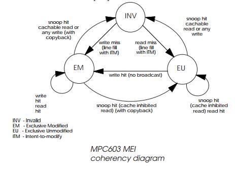
The MPC603 uses this simplified form of protocol to sup-port other
intelligent bus masters such as DMA controllers. It is not as good as the MESI
bus for true multiprocessor support. On the other hand, it is less complex and
easier to implement. The three states are defined as follows:
Invalid The
target address is not cached.
Exclusive unmodified The target address is in the cache but the data is coherent with system memory.
Exclusive modified The target address is in the cache, but the contents have been modified and are not coherent with system
memory. No other cache in the system has this data.
Note that the cache coherency implementation is processor specific and
may change. The two mechanisms described here are the two most commonly used
methods for processors and are likely to form the basis of future designs.
Two final points: these schemes require information to be passed by the
external buses to allow other bus masters to identify the transitions. This
requires the hardware design to implement them. If this is not done, these
schemes will not work and the software environment may require extensive change
and the imposition of constraints. Cache coherency may need to be re-stricted
to cache inhibited or write-through. DMA accesses could only be made to cache
inhibited memory regions. The supervisor must take responsibility for these
decisions and implementations to ensure correct operation. In other words, do
not assume that cache coherency software for one hardware design will work on
another. It will, if the bus interface design is the same. It will not if they
are different.
Finally, cache coherency also means identifying the areas of memory
which are not to be cached.
Burst interfaces
The adoption of burst interfaces by virtually all of today’s high
performance processors has led to the development of special memory interfaces
which include special address generation and data latches to help the designer.
Burst interfaces take advantage of page and nibble mode memories which supply
data on the first access in the normal time, but can supply subsequent data far
quicker.
The burst interface, which is used on processors from Motorola, Intel,
AMD, MIPs and many other manufacturers gains its performance by fetching data
from the memory in bursts from a line of sequential locations. It makes use of
a burst fill technique where the processor will access typically four words in
succession, enabling a complete cache line to be fetched or written out to memory.
The improved speed is obtained by taking advantage of page mode or static
column memory. These type of memories offer faster access times — single cycle
in many cases — after the initial access is made.
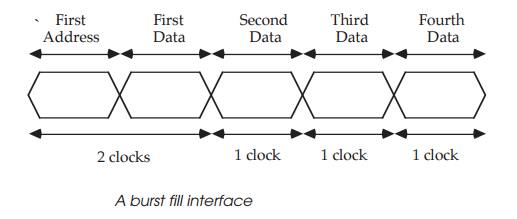
The advantage is a reduction in clock cycles needed to fetch the same
amount of data. To fetch four words with a three clock memory cycle takes 12
clocks. Fetching the same amount of data using a 2-1-1-1 burst (two clocks for
the first access, single cycles for the remainder) takes only five clocks. This
type of interface gives a good fit with the page mode DRAM where the first
access is used to set up the page access and the remainder of the burst
accesses addresses within the page, thus taking advantage of the faster access.
Burst fill offers advantages of faster and more efficient memory
accesses, but there are some fundamental changes in its operation when compared
with single access buses. This is par-ticularly so with SRAM when it is used as
part of a cache:
•
The address is only supplied for
the first access in a burst and not for the remaining accesses. External logic
is re-quired to generate the additional addresses for the memory interface.
•
The timing for each data access
in the burst sequence is unequal: typical clock timings are 2-1-1-1 where two
clocks are taken for the first access, but subsequent accesses are single
cycle.
•
The subsequent single cycle
accesses compress address generation, set-up and hold and data access into a
single cycle, which can cause complications generating write pulses to write
data into the SRAM, for example.
These characteristics lead to conflicting criteria within the interface:
during a read cycle, the address generation logic needs to change the address
to meet set-up and hold times for the next access, while the current cycle
requires the address to remain constant during its read access. With a write
cycle, the need to change the address for the next cycle conflicts with the
write pulse and constant address required for a successful write.
Meeting the interface needs
For a designer implementing such a system there are four methods of
improving the SRAM interface and specification to meet the timing criteria:
•
Use faster memory.
•
Use synchronous memory with
on-chip latches to reduce gate delays.
•
Choose parts with short write
pulse requirements and data set-up times.
•
Integrate address logic on-chip
to remove the delays and give more time.
While faster and faster memories are becoming available, they are more
expensive, and memory speeds are now becoming limited by on- and off-chip
buffer delays rather than the cell access times. The latter three methods
depend on semiconductor manu-facturers recognising the designer’s difficulties
and providing static RAMs which interface better with today’s high performance
processors.
This approach is beneficially for many high speed proces-sors, but it is
not a complete solution for the burst interfaces. They still need external
logic to generate the cyclical addresses from the presented address at the
beginning of the burst memory access. This increases the design complexity and
forces the use of faster memories than is normally necessary simply to cope
with the propagation delays. The obvious step is to add this logic to the
latches and registers of a synchronous memory to create a protocol specific
memory that supports certain bus protocols. The first two members of Motorola’s
protocol specific products are the MCM62940 and MCM62486 32k × 9 fast static RAMs. They are, as their part numbering suggests,
designed to support the MC68040 and the Intel 80486 bus burst protocols. These
parts offer access times of 15 and 20 ns.
The first access may take two processor clocks but remain-ing accesses
can be made in a single cycle. There are some restric-tions to this: the
subsequent accesses must be in the same memory page and the processor must have
somewhere to store the extra data that can be collected. The obvious solution
is to use this burst interface to fill a cache line. The addresses will be in
the same page and by storing the extra data in a cache allows a processor to
use it at a later date without consuming additional bus bandwidth. The main
problem faced by designers with these interfaces is the generation of the new
addresses. In most designs the processor will only issue the first address and
will hold this constant during the extra accesses. It is up to the interface
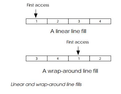
logic to take this address and increment it with every access. With processors
like the MC68030, this function is a straight incremental count. With the
MC68040, a wrap-around burst is used where the required data is fetched first
and the rest of the line fetched, wrapping around to the line beginning if
necessary. Although more efficient for the processor, the wrap-around logic is
more complicated.
The solution is to add this logic along with latches and registers to a
memory to create a specific part that supports certain bus protocols. The first
two members of Motorola’s protocol specific products are the MCM62940 and
MCM62486 32k × 9 fast static RAMs. They are, as their part numbering suggests,
designed to support the MC68040 and the Intel 80486 bus burst protocols. These
parts offer access times of 15 and 20 ns.
The MCM62940 has an on-chip burst counter that exactly matches the
MC68040 wrap-around burst sequence. The address and other control data can be
stored either by using the asynchro-nous or synchronous signals from the
MC68040 depending on the design and its needs. A late write abort is supported
which is useful in cache designs where cache writes can be aborted later in the
cycle than normally expected, thus giving more time to decide whether the
access should result in a cache hit or be delayed while stale data is copied
back to the main system memory.
The MCM62486 has an on-chip burst counter that exactly matches the Intel
80486 burst sequence, again removing external logic and time delays and
allowing the memory to respond to the processor without the need for the wait
state normally inserted at the cycle start. In addition, it can switch from
read to write mode while maintaining the address and count if a cache read miss
occurs, allowing cache updating without restarting the whole cycle.
Related Topics