Chapter: Embedded Systems Design : Memory systems
Memory systems and Memory technologies
Memory systems
Within any embedded system, memory is an important part of the design,
and faced with the vast variety of memory that is available today, choosing and
selecting the right type for the right application is of paramount importance.
Today's designs use more than just different types of memory and will include
both memory management and memory protection units to partition and isolate the
memory system. Memory caches are used to keep local copies of data and code so
that it is accessed faster and does not delay the processor. As a result, the
memory subsystem has become extremely complex. Designs only seen on mainframes
and supercomputers are now appearing on the humble embedded processor. This
chapter goes through the different types that are available and discusses the
issues associated with them that influence the design.
Memory technologies
Within any embedded system design that uses external memory, it is
almost a sure bet that the system will contain a mixture of non-volatile memory
such as EPROM (erasable pro-grammable read only memory) to store the system
software and DRAM (dynamic random access memory) for use as data and additional
program storage. With very fast systems, SRAM (static random access memory) is
often used as a replacement for DRAM because of its faster speed or within
cache memory subsystems to help improve the system speed offered by DRAM.
The main signals used with memory chips fall into several groups:
•
Address bus
The address bus is used to select the particular location within the memory
chip. The signals may be multiplexed as in the case with DRAM or
non-multiplexed as with SRAM.
•
Data bus
This bus provides the data to and from the chip. In some cases, the
memory chip will use separate pins for incoming and outgoing data, but in others
a single set of pins is used with the data direction controlled by the status
of chip select signals, the read/write pin and output enable pins.
•
Chip selects
These can be considered as additional address pins that are used to
select a specific chip within an array of memory devices. The address signals
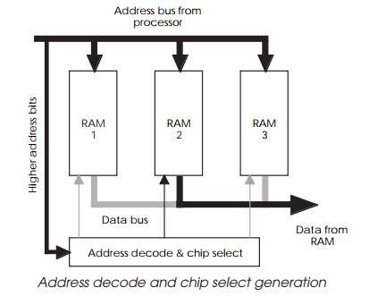
that are used for the chip selects are normally the higher order pins. In the
example shown, the address decode logic has enabled the chip select for the
second RAM chip — as shown by the black arrow — and it is therefore the only
chip driving the data bus and supplying the data. As a result, each RAM chip is
located in its own space within the memory map although it shares the same
address bus signals with all the other RAM chips in the array.
•
Control signals including
read/write signals
Depending on the functionality provided by the memory device, there are
often additional control signals. Random access memory will have a read/write
signal to indicate the type of access. This is missing from read only devices
such as EPROM. For devices that have multiplexed address buses, as in the case
with DRAM, there are control signals associated with this type of operation.
There are now several different types of semiconductor memory available
which use different storage methods and have different interfaces.
DRAM technology
DRAM is the predominantly used memory technology for PCs and embedded
systems where large amounts of low cost memory are needed. With most memory
technologies, the cost per bit is dependent on two factors: the number of
transistors that are used to store each bit of data and the type of package
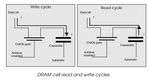
that is used. DRAM achieves its higher density and lower cost because it only
uses a single transistor cell to store each bit of data. The data storage
element is actually a small capacitor whose voltage repre-sents a binary zero
or one which is buffered by the transistor. In comparison, a SRAM cell contains
at least four or five transistors to store a single bit of data and does not
use a capacitor as the active storage element. Instead, the transistors are
arranged to form a flip-flop logic gate which can be flipped from one binary
state to the other to store a binary bit.
DRAM technology does have its drawbacks with the major one being its
need to be refreshed on a regular basis. The term ‘dynamic’ refers to the
memory’s constant need for its data to be refreshed. The reason for this is
that each bit of data is stored using a capacitor, which gradually loses its
charge. Unless it is fre-quently topped up (or refreshed), the data disappears.
This may appear to be a stupid type of memory — but the advantage it
offers is simple — it takes only one transistor to store a bit of data whereas
static memory takes four or five. The memory chip’s capacity is dependent on
the number of transistors that can be fabricated on the silicon and so DRAM
offers about four times the storage capacity of SRAM (static RAM). The refresh
overhead takes about 3–4% of the theoretical maximum processing available and
is a small price to pay for the larger storage capacity. The refresh is
performed automatically either by a hardware controller or through the use of
software. These techniques will be described in more detail later on in this
chapter.
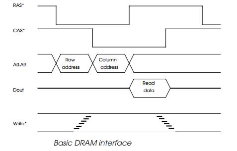
The basic DRAM interface takes the processor generated address, places
half of the address (the high order bits) onto the memory address bus to form
the row address and asserts the RAS* signal. This partial address is latched
internally by the DRAM. The remaining half (the low order bits), forming the
column address, are then driven onto the bus and the CAS* signal asserted.
After the access time has expired, the data appears on the Dout pin and is
latched by the processor. The RAS* and CAS* signals are then negated. This
cycle is repeated for every access. The majority of DRAM specifications define
minimum pulse widths for the RAS* and CAS* and these often form the major part
in defining the memory access time. When access times are quoted, they usually
refer to the time from the assertion of the RAS* signal to the appearance of
the data. There are several variations on this type of interface, such as page
mode and EDO. These will be explained later on in this chapter
Video RAM
A derivative of DRAM is the VRAM (video RAM), which is essentially a
DRAM with the ability for the processor to update its contents at the same time
as the video hardware uses the data to create the display. This is typically
done by adding a large shift register to a normal DRAM. This register can be
loaded with a row or larger amounts of data which can then be serially clocked
out to the video display. This operation is in parallel with normal read/ write
operations using a standard address/data interface.
Related Topics