Chapter: 11th 12th std standard Class Physics sciense Higher secondary school College Notes
Single stage CE amplifier
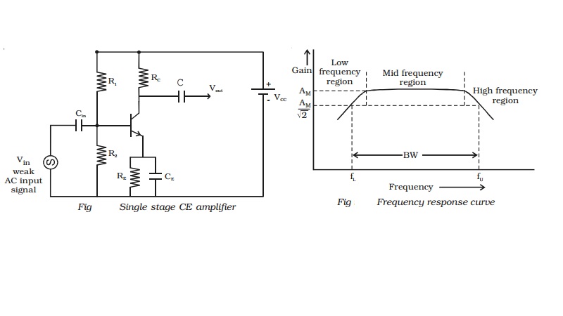
Single stage CE amplifier
Fig shows a single stage CE amplifier. The
different circuit elements and their functions are described as follows.
(i) Biasing circuit : The
resistances R1, R2 and RE form the biasing and
stabilization circuit.
(ii)Input capacitance Cin : This is used to
couple the signal to the base of the transistor. If this is not used, the
signal source resistance will come across R2 and thus change the
bias. The capacitor Cin allows only a.c. signal to flow.
(iii) Emitter bypass capacitor CE
: This is connected in parallel with RE to provide a low reactance
path to the amplified a.c. signal. If it is not used, then amplified a.c.
signal flowing through RE will cause a voltage drop across it,
thereby shifting the output voltage.
(iv)Coupling capacitor C : This is used to couple the
amplified signal to the output device. This capacitor C allows only a.c. signal
to flow.
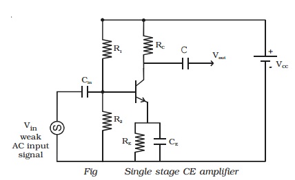
Working
When a weak input a.c. signal is applied to the base of the
transistor, a small base current flows. Due to transistor action, a much larger
a.c. current flows through collector load RC, a large voltage
appears across RC and hence at the output. Therefore, a weak signal
applied to the base appears in amplified form in the collector circuit. Voltage
gain (Av) of the amplifier is the ratio of the amplified output
voltage to the input voltage.
Frequency response and bandwidth
The voltage gain (Av) of the amplifier for different input
frequencies can be determined. A graph can be drawn by taking frequency (f)
along X-axis and voltage gain (Av) along Y-axis. The frequency
response curve obtained will be of the form as shown in Fig. It can be seen
that the gain decreases at very low and very high frequencies, but it remains
constant over a wide range of mid-frequency region.
Lower cut off frequency (fL ) is defined as the frequency in the
low 1
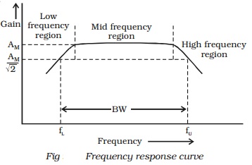
frequency range at which the gain of the amplifier is 2 times the mid frequency gain (AM).
Upper cut off frequency (fU) is defined as the frequency in the high
frequency range at which the gain of the amplifier is 1/rt(2) times the mid
frequency gain (AM).
Bandwidth is
defined as the frequency interval between lower cut off and upper cut off
frequencies.
BW = fU
- fL
Related Topics