Chapter: Embedded Systems Design : Memory systems
MC68000 asynchronous bus - interfaces
MC68000 asynchronous bus - interfaces
The MC68000 bus is fundamentally different to the buses used on the
MC6800 and MC6809 processors. Their buses were synchronous in nature and
assumed that both memory and pe-ripherals could respond within a cycle of the
bus. The biggest drawback with this arrangement concerned system upgrading and
compatibility. If one component was uprated, the rest of the system needed
uprating as well. It was for this reason that all M6800 parts had a system
rating built into their part number. If a design specified an MC6809B, then it
needed 2 MHz parts and subsequently, could not use an ‘A’ version which ran at
1 MHz. If a design based around the 1 MHz processor and peripherals was
upgraded to 2 MHz, all the parts would need replacing. If a peripheral was not
available at the higher speed, the system could not be upgraded. With the
increasing processor and memory speeds, this restriction was unacceptable.
The MC68000 bus is truly asynchronous: it reads and writes data in
response to inputs from memory or peripherals which may appear at any stage
within the bus cycle. Provided certain signals meet certain set-up times and
minimum pulse widths, the proces-sor can talk to anything. As the bus is truly
asynchronous it will wait indefinitely if no reply is received. This can cause
similar symptoms to a hung processor; however, most system designs use a
watchdog timer and the processor bus error signal to resolve this problem.
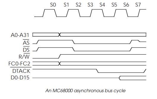
A typical bus cycle starts with the address, function codes and the
read/write line appearing on the bus. Officially, this data is not valid until
the address strobe signal AS* appears but many designs start decoding prior to
its appearance and use the AS* to validate the output. The upper and lower data
strobes, together with the address strobe signal (both shown as DS*), are
asserted to indicate which bytes are being accessed on the bus. If the upper
strobe is asserted, the upper byte is selected. If the lower strobe is
asserted, the lower byte is chosen. If both are asserted together, a word is
being accessed.
Once complete, the processor waits until a response ap-pears from the
memory or peripheral being accessed. If the rest of the system can respond
without wait states (i.e. the decoding and access times will be ready on time)
a DTACK* (Data Transfer ACKnowledge) signal is returned. This occurs slightly
before clock edge S4. The data is driven onto the bus, latched and the address
and data strobes removed to acknowledge the receipt of the DTACK* signal by the
processor. The system responds by removing DTACK* and the cycle is complete. If
the DTACK* signal is delayed for any reason, the processor will simply insert
wait states into the cycle. This allows extra time for slow memory or
peripherals to prepare data.
The advantages that this offers are many fold. First, the processor can
use a mixture of peripherals with different access speeds without any
particular concern. A simple logic circuit can generate DTACK* signals with the
appropriate delays as shown. If any part of the system is upgraded, it is a
simple matter to adjust the DTACK* generation accordingly. Many M68000 boards
pro-vide jumper fields for this purpose and a single board and design can
support processors running at 8, 10, 12 or 16 MHz. Secondly, this type of
interface is very easy to interface to other buses and peripherals. Additional
time can be provided to allow signal translation and conversion.
Related Topics