Chapter: Embedded Systems Design : Memory systems
Bank switching and Memory overlays
Bank switching
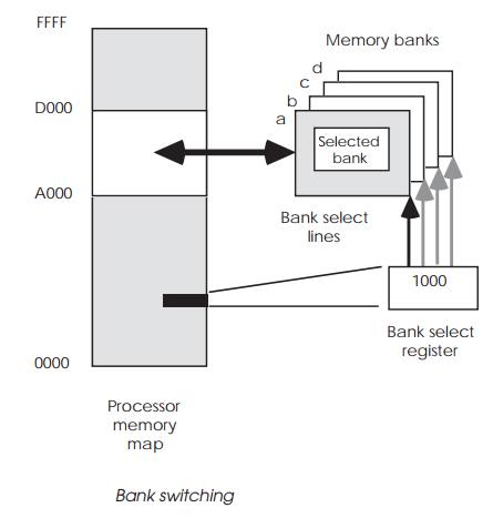
Bank switching simply involves having several banks of memory with the
same address locations. At any one time, only one bank of memory is enabled and
accessible by the microproc-essor. Bank selection is made by driving the
required bank select line. These lines come from either an external parallel
port or latch whose register(s) appear as a bank switching control register
within the processors’s normal address map.
In the example, the binary value 1000 has been loaded into the bank
selection register. This asserts the select line for bank ‘a’ which is
subsequently accessed by the processor. Special VLSI (very large scale
integration) parts were even developed which provided large number of banks and
additional control facilities: the Motorola MC6883 SAM is an example used in
the Dragon MC6809-based home computer from the early 1980s.

Memory overlays
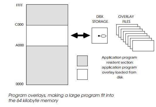
Program overlays are similar to bank switching except that some form of
mass storage is used to contain the different over-lays. If a particular
subroutine is not available, the software stores part of its memory as a file
on disk and loads a new program section from disk into its place. Several
hundred kilobytes of program, divided into smaller sections, can be made to
overlay a single block of memory.

This whole approach requires careful design so that the system integrity
is ensured. Data passing between the overlays can be a particular problem which
requires careful design. Typi-cally, data is passed and stored either on the
processor stack or in reserved memory which is locked in and does not play any
part in the overlay process, i.e. it is resident all the time.
Related Topics