Chapter: Television and Video Engineering : Fundamentals of Television
Vidicon
VIDICON
The Vidicon came into general use in the early 50’s and gained immediate popularity because of its small size and ease of operation. It functions on the principle of photoconductivity, where the resistance of the target material shows a marked decrease when exposed to light. illustrates the structural configuration of a typical vidicon, and Fig.
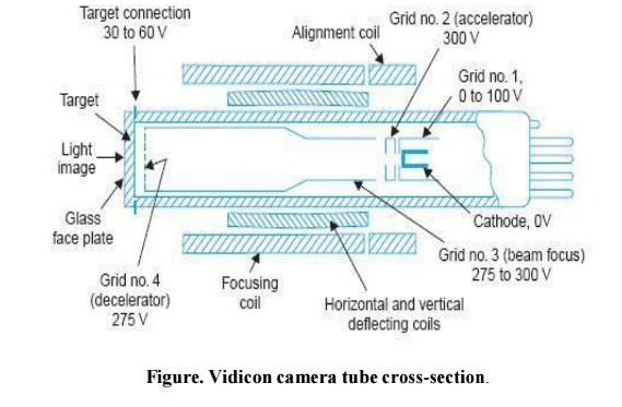
Shows the circuit arrangement for developing camera signal output. As shown there, the target consists of a thin photo conductive layer of either selenium or anti-mony compounds.
This is deposited on a transparent conducting film, coated on the inner surface of the face plate. This conductive coating is known as signal electrode or plate. Image side of the photolayer, which is in contact with the signal electrode, is connected to DC supply through the load resistance RL.
The beam that emerges from the electron gun is focused on surface of the photo conductive layer by combined action of uniform magnetic field of an external coil and electrostatic field of grid No 3. Grid No. 4 provides a uniform decelerating field between itself, and the photo conductive layer, so that the electron beam approaches the layer with a low velocity to prevent any secondary emission.
Deflection of the beam, for scanning the target, is obtained by vertical and horizontal deflecting coils, placed around the tube.
Charge Image
The photo layer has a thickness of about 0.0001 cm, and behaves like an insulator with a resistance of approximately 20 MΩ when in dark. With light focused on it, the photon energy enables more electrons to go to the conduction band and this reduces its resistivity.
When bright light falls on any area of the photoconductive coating, resistance across the thickness of that portion gets reduces to about 2 MΩ. Thus, with an image on the target, each point on the gun side of the photo layer assumes a certain potential with respect to the DC supply, depending on its resistance to the signal plate.
For example, with a B + source of 40 V (see Fig), an area with high illumination may attain a potential of about + 39 V on the beam side. Similarly dark areas, on account of high resistance of the photo layer may rise to only about + 35 volts.
Thus, a pattern of positive potentials appears, on the gun side of the photo layer,
producing a charge image, that corresponds to the incident optical image.
Storage Action
Though light from the scene falls continuously on the target, each element of the photo coating is scanned at intervals equal to the frame time. This results in storage action and the net change in resistance, at any point or element on the photoconductive layer, depends on the time, which elapses between two successive scanning and the intensity of incident light.
Since storage time for all points on the target plate is same, the net change in resistance of all elementary areas is proportional to light intensity variations in the scene being televised. Signal Current As the beam scans the target plate, it encounters different positive potentials on the side of the photo layer that faces the gun.
Sufficient number of electrons from the beam are then deposited on the photo layer surface to reduce the potential of each element towards the zero cathode potential. The remaining electrons, not deposited on the target, return back and are not utilized in the vidicon.
However, the sudden change in potential on each element while the beam scans, causes a current flow in the signal electrode circuit producing a varying voltage across the load resistance R L. Obviously, the amplitude of current and the consequent output voltage across R L are directly proportional to the light intensity variations on the scene.
Note that, since, a large current would cause a higher voltage drop across R L , the output voltage is most negative for white areas. The video output voltage, that thus develops across the load resistance (50 K-ohms) is adequate and does not need any image or signal multiplication as in an image orthicon.
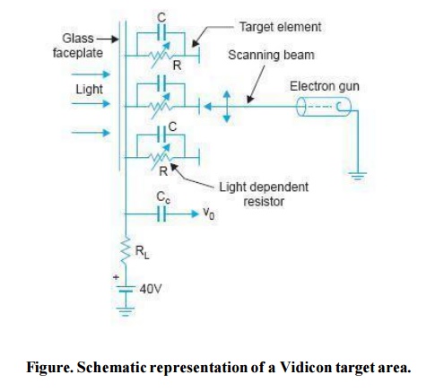
The output signal is further amplified by conventional amplifiers before it leaves the camera unit. This makes the vidicon a much simpler picture tube. Leaky Capacitor Concept Another way of explaining the development of ‘charge image’ on the photo layer is to consider it as an array of individual target elements, each consisting of a capacitor paralleled with a light dependent resistor. A number of such representations are shown in Fig.
As seen there, one end of these target elements is connected to the signal electrode and the other end is unterminated facing the beam. In the absence of any light image, the capacitors attain a charge almost equal to the B + (40 V) voltage in due course of time.
However, when an image is focused on the target the resistors in parallel with the capacitors change in value depending on the intensity of light on each unit element.
For a high light element, the resistance across the capacitor drops to a fairly low value, and this permits lot of charge from the capacitor to leak away. At the time of scanning, more electrons are deposited, on the unterminated end of this capacitor to recharge it to the full supply voltage of + 40 V. The consequent flow of current that completes its path through R L develops a signal voltage across it.
Similarly for black areas of the picture, the resistance across the capacitors remains fairly high, and not much charge is allowed to leak from the corresponding capacitors. This in turn needs fewer number of electrons from the beam to recharge the capacitors. The resultant small current that flows, develops a lower voltage across the load resistance.
The electron beam thus ‘sees’ the charge on each capacitor, while scanning the target, and delivers more or less number of electrons to recharge them to the supply voltage. This process is repeated every 40 ms to provide the necessary video signal corresponding to the picture details at the upper end of the load resistor.
The video signal is fed through a blocking capacitor to an amplifier for necessary amplification.
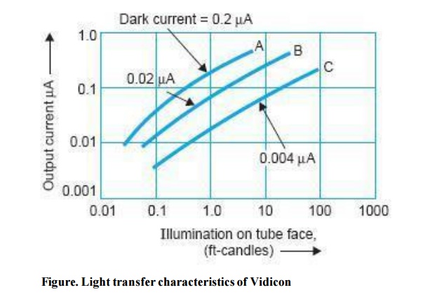
Light Transfer Characteristics
Vidicon output characteristics are shown in Fig. Each curve is for a specific value of ‘dark’ current, which is the output with no light. The ‘dark’ current is set by adjusting the target voltage.
Sensitivity and dark current both increase as the target voltage is increased.
Typical output for the vidicon is 0.4 μA for bright light with a dark current of 0.02 μA. The photoconductive layer has a time lag, which can cause smear with a trail following fast moving objects.
The photoconductive lag increases at high target voltages, where the vidicon has its highest sensitivity.
Applications
Earlier types of vidicons were used only where there was no fast movement, because of inherent lag. These applications included slides, pictures, closed circuit TV etc. The present day improved vidicon finds wide applications in education, medicine, industry, aerospace and oceanography.
It is, perhaps, the most popular tube in the television industry. Vidicon is a short tube with a length of 12 to 20 cm and diameter between 1.5 and 4 cm. Its life is estimated to be between 5000 and 20,000 hours.
Related Topics