Chapter: Television and Video Engineering : Fundamentals of Television
Silicon Diode Array Vidicon
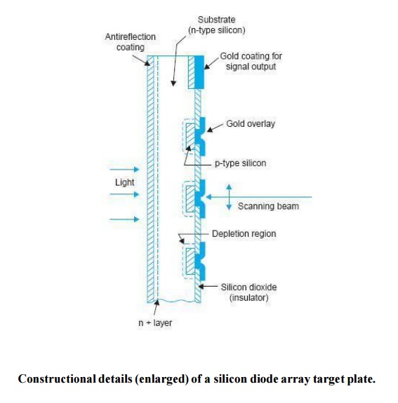
SILICON DIODE ARRAY VIDICON
This is another variation of vidicon where the target is prepared from a thine n-type silicon wafer instead of deposited layers on the glass faceplate. The final result is an array of silicon photodiodes for the target plate. Figure shows constructional details of such a target. As shown there, one side of the substrate (n-type silicon) is oxidized to form a film of silicon dioxide (SiO 2 ) which is an insulator.
Then by photo masking and etching processes, an array of fine openings is made in the oxide layer. These openings are used as a diffusion mask for producing corresponding number of individual photodiodes.
Boron, as a dopant is vaporized through the array of holes, forming islands of p-type silicon on one side of the n-type silicon substrate. Finally a very thin layer of gold is deposited on each p-type opening to form contacts for signal output.
The other side of the substrate is given an antireflection coating. The resulting p-n photodiodes are about 8 μm in diameter. The silicon target plate thus formed is typically 0.003 cm thick, 1.5 cm square having an array of 540 × 540 photodiodes. This target plate is mounted in a vidicon type of camera tube.
Scanning and Operation
The photodiodes are reverse biased by applying +10 V or so to the n + layer on the substrate. This side is illuminated by the light focused on to it from the image. The incidence of light generates electron-hole pairs in the substrate. Under influence of the applied electric field, holes are swept over to the ‘p’ side of the depletion region thus reducing reverse bias on the diodes.
This process continues to produce storage action till the scanning beam of electron gun scans the photodiode side of the substrate. The scanning beam deposits electrons on the p-side thus returning the diodes to their original reverse bias.
The consequent sudden increase in current across each diode caused by the scanning beam represents the video signal. The current flows through a load resistance in the battery circuit and develops a video signal proportional to the intensity of light falling on the array of photodiodes.
A typical value of peak signal current is 7 μA for bright white light. The vidicon employing such a multi diode silicon target is less susceptible to damage or burns due to excessive high lights. It also has low lag time and high sensitivity to visible light which can be extended to the infrared region.
A particular make of such a vidicon has the trade name of ‘Epicon’. Such camera tub es have wide applications in industrial, educational and CCTV (closed circuit television) services.
Related Topics