Chapter: Television and Video Engineering : Fundamentals of Television
Solid State Image Scanners
SOLID STATE IMAGE SCANNERS
The operation of solid state image scanners is based on the functioning of charge coupled devices (CCDs) which is a new concept in metal-oxide-semiconductor (MOS) circuitry.
The CCD may be thought of to be a shift register formed by a string of very closel y spaced MOS capacitors. It can store and transfer analog charge signals—either electrons or holes—that may be introduced electrically or optically. The constructional details and the manner in which storing and transferring of charge occurs is illustrated in Fig.
he chip consists of a p-type substrate, the one side of which is oxidized to form a film of silicon dioxide, which is an insulator. Then by photolithographic processes, similar to those used in miniature integrated circuits an array of metal electrodes, known as gates, are deposited on the insulator film.
This results in the creation of a very large number of tiny MOS capacitors on the entire surface of the chip. The application of small positive potentials to the gate electrodes results in the development of depletion regions just below them.
These are called potential wells. The depth of each well (depletion region) varies with the magnitude of the applied potential. As shown in Fig. (a),
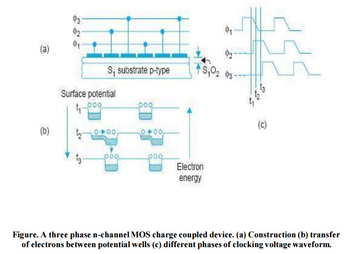
The gate electrodes operate in groups of three, with every third electrode connected to a common conductor. The spots under them serve as light sensitive elements.
When any image is focused onto the silicon chip, electrons are generated within it, but very close to the surface. The number of electrons depends on the intensity of incident light. Once produced they collect in the nearby potential wells. As a result the pattern of collected charges represents the optical image.
Charge Transfer
The charge of one element is transferred along the surface of the silicon chip by appl ying a more positive voltage to the adjacent electrode or gate, while reducing the voltage on it. The minority carriers (electrons in this case) while accumulating in the so called wells reduce their depths much like the way a fluid fills up in a container.
The accumulation of charge carries under the first potential wells of two consecutive trios is shown in Fig. (b) Where at instant t 1 a potential φ 1 exists at the corresponding gate electrodes. In practice the charge transfer is effected by multiphase clock voltage pulses (see Fig. 6.12 (c)) which are applied to the gates in a suitable sequence.
The manner in which the transition takes place from potential wells under φ 1 to those under φ 2 is illustrated in Fig. (b). A similar transfer moves charges from φ 2 to φ 3 and then from φ 3 to φ 1 under the influence of continuing clock pulses.
Thus, after one complete clock cycle, the charge pattern moves one stage (three gates) to the right. The clocking sequence continues and the charge finally reaches the end of the array where it is collected to form the signal current.
Scanning of Television Pictures
A large number of CCD arrays are packed together to form the image plate. It does not need an electron gun, scanning beam, high voltage or vacuum envelope of a conventional camera tube.
The potential required to move the charge is only 5 to 10 volt. The spot under each trio serves as the resolution cell. When light image is focused on the chip, electrons are generated in proportion to the intensity of light falling on each cell.

Figure. Basic organization of line addressed charge transfer area imaging devices.
The principle of one-dimensional charge transfer as explained above can be integrated in various ways to render a solid-state area image device. The straightforward approach consists of arranging a set of linear imaging structures so that each one corresponds to a scan line in the display.
The lines are then independently addressed and read into a common output diode by application of driving pulses through a set of switches controlled by an address register as shown in Fig To reduce capacitance, the output can be simply a small diffused diode in one corner of the array.
The charge packets emerging from any line are carried to this diode by an additional vertical output register. In such a line addressed structure (Fig.) where the sequence of addressing the lines is determined by the driving circuitry, interlacing can be accomplished in a natural way.
Cameras Employing Solid-State Scanners
CCDs have a bright future in the field of solid state imaging. Full TV line-scan arrays have already been constructed for TV cameras. However, the quality of such sensors is not yet suitable for normal TV studio use.
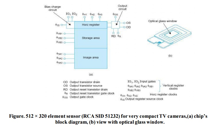
RCA SID 51232 is one such 24 lead dual-in-line image sensor. It is a self-scanned sensor intended primarily for use in generating standard interlaced 525 line television pictures. The device contains 512 × 320 elements and is constructed with a 3 phase n-channel, vertical frame transfer organization using a sealed silicon gate structure.
Its block diagrams is shown in Fig. (a). The image scanner’s overall picture performance is comparable to that 2/3 inch vidicon camera tubes but undesirable characteristics such as lag and micro phonics are eliminated. The SID 51232 is supplied in a hermetic, edge contacted, 24-connection ceramic dual-inline package. The package contains an optical glass window (see Fig. (b)) which allows an image to be focused into sensor’s 12.2 mm image diagonal.
Related Topics