Chapter: Embedded Systems Design : Basic peripherals
UART implementations
UART implementations
8250/16450/16550
Probably the most commonly known and used UART is the 8250 and its
derivatives as used to provide serial ports COM1
and COM2 on an IBM PC. The original
design used an Intel 8250 which has
been largely replaced by the National Semiconductor 16450 and 16550 devices or
by cloned devices within a super I/O chip which combines all the PC’s I/O devices
into a single piece of silicon.
The original devices used voltage level shifters to provide the + and
–12 volt RS232 signalling voltage levels but this function is sometimes
included within the UART as well.
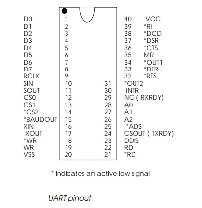
The pinout shows the hardware signals that are used and these fall into
two groups: those that are used to provide the UART interface to the processor
and those that are the UART signals. Some of the signals are active low, i.e.
when they are at a zero voltage level, they represent a logical one. These
signals are indicated by an asterisk.
The interface signals
The UART interface signals are for the 8250 UART and its derivatives are
as follows:
*ADS This is the address strobe signal
and is used to latch the address and chip select signals during a processor
access. The latching takes place on the positive edge of the and assumes that
the other signals are stable at this point. This signal can be ignored by
permanently asserting it. In this case, the address and chip selects must be
set up and stable for the whole cycle with the processor and peripheral clock
signals providing the timing references. The IBM PC uses the chip in this way.
*BAUDOUT This is the 16x clock signal from
the transmitter section of the UART. The clock frequency is the main clock
frequency divided by the values stored in the baud generator divisor latches.
It is normally used — as in the IBM PC, for example — to route the transmit
clock back into the receive section by connecting this pin to the RCLK pin. By
doing this, both the transmit and receive baud rates are the same and use the
same clock frequency. To create an asynchronous system such as 1200/75 which is
used for teletext links, an external transmit clock is used to feed RCLK
instead.
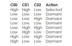
CS0,1 and 2 These
signals are used to select the UART and are derived from the rest of the
processor’s address signals. The lower 3 bits of the CPU address bus are
connected to the A0–A2 pins to select the internal registers. The rest of the
address bus is decoded to generate a chip select signal. This can be a single
entity, in which case two of the chip selects are tied to the appropriate logic
level. If the signal is low, then CS0 and CS1 would be tied high. The provision
of these three chip selects provides a large amount of flexibility. The truth
table is shown below.
D0–D7 These signals form the 8 bit bus
that is connected between the peripheral and the processor. All transfers between the UART and processor are byte based.
DDIS This goes low whenever the CPU is
reading data from the UART. It can be used to control bus arbitration logic.
INTR This pin is normally connected to
an interrupt pin on the processor or in the case of the IBM PC, the interrupt
controller. It is asserted when the UART needs data to be transferred to or
from the internal buffers, or if an error condition has occurred such as a data
overrun. The ISR has to investigate the UART’s status registers to determine
the actual service(s) requested by the peripheral.
MR This is the master reset pin and
is used to reset the device and restore the internal registers to their
power-on default values. This is normally connected to the system/processor
reset signal to ensure that the UART is reset when the system is.
*OUT1 This is a general-purpose I/O pin
whose state can be set by programming bit 2 of the MCR to a ‘1’.
*OUT2 This is another general-purpose
I/O pin whose state can be set by programming bit 3 of the MCR ‘1’. In the IBM
PC it is used to gate the interrupt signal from the UART to the interrupt
controller. In this way, interrupts from the UART can be externally disabled.
RCLK This is the input for the clock
for the receiver section of the chip. See *BAUDOUT on the previous page for more details.
RD, *RD These are read strobes that are
used to indicate the type of access that the CPU needs to perform. If RD is
high or *RD is low, the CPU access is a read cycle.
SIN This is the serial data input pin
for the receiver.
SOUT This is the serial data output
pin for the transmitter.
*RXRDY,*TXRDY These pins are used for additional DMA control and can be used to
initiate DMA transfers to and from the read and write buffers. They are not
used within the IBM PC design where the CPU is responsible for moving data to and
from the UART.
WR, *WR These are read strobes that are
used to indicate the type of access
that the CPU needs to perform. If WR is high or *WR is low, the CPU access is a
write cycle.
XIN, XOUT These
pins are used to either connect an external crystal or connect to an external
clock. The frequency is typically 8 MHz.
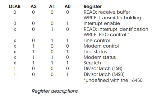
A0–2 These are the three address
signals which are used in conjunction with DLAB to select the internal
registers. They are normally connected to the lower bits of the processor address
bus. The upper bits are normally decoded to create a set of chip select signals
to select the UART and locate it at a specific address location.
The main difference between the various devices concerns the buffer size
that they support and, in particular, the effect that it has on the effective
throughput of the UART.
The UART relies on the CPU to transfer data and therefore the limit on
the serial data throughput that can be sustained is determined by the time it
takes to interrupt the CPU and for the appropriate interrupt service routine to
identify the reason for the interrupt — it may have been raised as a result of
an error — and then transfer the data if the interrupt corresponds to a data
ready for transfer request. Finally, the processor returns from the inter-rupt.
The time to perform this task is determined by the processor type and
memory speed. The time then defines the maximum rate that data can be received.
If the interrupt service routine takes longer than the time to receive the next
data, there is a large risk that a data overrun will occur where data is
received before the previous byte is read by the processor. To address this
issue, a buffer is often used. With the later versions of the UART such as the 16450
and 16550, the FIFO buffer size has been increased. The largest buffer (16
bytes) is available on the 16550 and this device is frequently used for high
speed data communications.
The 16 byte buffer means that if the processor is late for the first byte,
any incoming data will simply be buffered and not cause a data overrun. As a
result, the interrupt service routine need only be executed 1/16 of the times
for a single buffer UART. This dramatically reduces the CPU processing needed
for high speed data transfer.
There is a downside: the data now arrives in a packet with up to 16
bytes and must be processed slightly differently. With a byte at a time, the
decoding of the data (i.e. is it a command or is it data that a higher level
protocol may impose?) is easy to decode. With a packet of up to 16 bytes, the
bytes have to be parsed to separate them out. This means that the decoding
software is slightly more complex to handle both the parsing and the
mecha-nisms to store and track the incoming data packets. An example of this in
included in the chapter on buffers.
The Motorola MC68681
Within the Motorola product offering, the MC68681 has become a fairly
standard UART that has been used in many MC680x0 designs. It has a quadruple
buffered receiver and a double buffered transmitter. The maximum transfer rates
that can be achieved are high: 9.8 Mbps with a 25 MHz clock with no clock
division (×1 mode) and 612 kbps with the same clock with a divide by 16 setting (×16 mode). Each transmitter and receiver is inde-pendently programmable
using one of 19 fixed rates.
It has a sophisticated interrupt structure that supports seven maskable
interrupt conditions:
•
Change of state on CTSx*
This is used to support hardware handshaking. If the CTS signal changes,
an interrupt can be generated to instruct the processor to stop or start
sending data. This fast response coupled with the buffering ensures that data
is not lost.
•
Break condition (either channel)
•
The break condition is either
used to request connection, i.e. send a break from a terminal to start a remote
login or is symptomatic of a lost or dropped connection.
•
Ready receive/FIFO full (either
channel)
As previously discussed, interrupts are ideal for the effi-cient
handling and control of receive buffers. This interrupt indicates that there is
data ready.
•
Transmitter ready (either
channel)
This is similar to the previous interrupt and is used to indicate that
the transmitter is ready to take data for trans-mission.
Related Topics