Chapter: Embedded Systems Design : Basic peripherals
I2C bus
I2C bus
The inter-IC, or I2C bus as it is more readily known, was developed by Philips originally
for use within television sets in the mid-1980s. It is probably the most known
simple serial interface currently used. It combines both hardware and software
protocols to provide a bus interface that can talk to many peripheral devices
and can even support multiple bus masters. The serial bus itself only uses two
pins for its implementation.
The bus consists of two lines called SDA and SCL. Both bus masters and
slave peripheral devices simply attach to these two lines as shown in the
diagram. For small numbers of devices and where the distance between them is
small, this connection can be direct. For larger numbers of devices and/or
where the track length is large, Philips can provide a special buffer chip
(P82B715) to increase the current drive.
The number of devices is effectively determined by the line length, clock
frequency and load capaci-tance which must not exceed 400 pF although derating
this to 200 pF is recommended. With low frequencies, connections of several
metres can be achieved without resorting to special drivers or buffers.
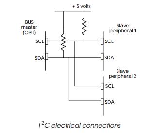
The drivers for the signals are bidirectional and require pull-up
resistors. When driven they connect the line to ground to create a low state.
When the drive is removed, the output will be pulled up to a high voltage to
create a high signal. Without the pull-up resistor, the line would float and
can cause indeterminate values and thus cause errors.
The SCL pin provides the reference clock for the transfer of data but it
is not a free running clock as used by many other serial ports. Instead it is
clocked by a combination of the master and slave device and thus the line
provides not only the clock but also a hardware handshake line.
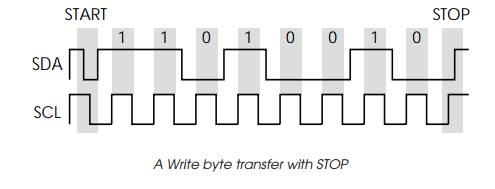
The SDA pin ensures the serial data is clocked out using the SCL line
status. Data is assumed to be stable on the SDA line if SCL is high and
therefore any changes occur when the SCL is low. The sequence and logic changes
define the three messages used.
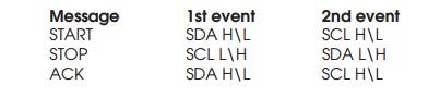
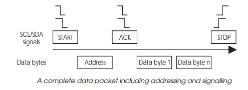
The table shows the hardware signalling that is used for the three
signals, START, STOP and ACKNOWLEDGE. The START and ACKNOWLEDGE signals are
similar but there is a slight difference in that the START signal is performed
entirely by the master whereas the ACKNOWLEDGE signal is a handshake between
the slave and master.
Data is transferred in packets with a packet containing one or more
bytes. Within each byte, the most significant bit is trans-mitted first. A
packet, or telegram as it is sometimes referred to, is defined as the data
transmitted between START and STOP signals sent from the master. Within the
packet transmission, the slave will acknowledge each byte by using the
ACKNOWLEDGE sig-nal. The basic protocol is shown in the diagram.
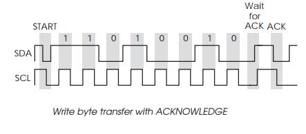
The ‘wait for ACK’ stage looks like another data bit except that it is
located as the ninth bit. With all data being transmitted as bytes, this extra
one bit is interpreted by the peripheral as an indication that the slave should
acknowledge the byte transfer. This is done by the slave pulling the SDA line
low after the master has released the data and clock line. The ACK signal is
physically the same as the START signal and is ignored by the other
periph-erals because the data packet has not been terminated by the STOP
command. When the ACKNOWLEDGE command is issued, it indicates that the transfer
has been completed. The next byte of data can start transmission by pulling the
SCL signal down low.
Read and write access
While the previous paragraphs described the general method of
transferring data, there are some specific differences for read and write
accesses. The main differences are concerned with who controls which line
during the handshake.
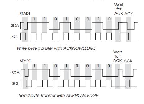
During a write access the sequence is as follows:
•
After the START and 8 bits have
been transmitted, the master releases the data line followed by the clock line.
At this point it is waiting for an acknowledgement.
•
The addressed slave will pull the
data line down to indicate the ACKNOWLEDGE signal.
•
The master will drive the clock
signal low and in return, the slave will release the data line, ready for the
first bit of the next byte to be transferred or to send a STOP signal.
During a read access the sequence is as follows:
•
After the 8 bits have been
transmitted by the slave, the slave releases the data line.
•
The master will now drive the
data line low.
•
The master will then drive the
clock line high and low to create a clock pulse.
•
The master will then release the
data line ready for the first bit of the next byte or a STOP signal.
It is also possible to terminate a transfer using a STOP instead of
waiting for an ACKNOWLEDGE. This is sometimes needed by some peripherals which
do not issue an ACKNOWL-EDGE on the last transfer. The STOP signal can even be
used in mid transmission of the byte if necessary.
Addressing peripherals
As mentioned before, the bus will support multiple slave devices. This
immediately raises the question of how the protocol selects a peripheral. All
the devices are connected onto the two signals and therefore can see all the
transactions that occur. The slave selection is performed by using the first
byte within the data packet as an address byte. The protocol works as shown in
the diagram. The master puts out the START signal and this tells all the
connected slave devices to start accepting the data. The ad-dress byte is sent
out and each slave device compares the address with its own value. If there is
a match, then it will send the ACKNOWLEDGE signal. If there is no match, then
there has been a programming error. In this case, there will be no ACKNOWL-EDGE
signal returned and effectively the SDA signal will remain high.
The address value is used to select the device and to indicate the type
of operation that the master requests: read if the eighth bit is set to one or
write if set to zero. This means that the address byte allows 128 devices with
read/write capability to be connected. The address value for a device is either
pre-programmed, i.e. assigned to that device number, or can be programmed
through the use of external pins. Care must be made to ensure that no two
devices have the same address.
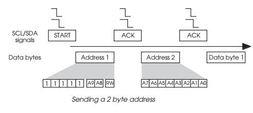
In practice, the number of available addresses is less be-cause some are
reserved and others are used as special commands. To provide more addressing,
an extended address has been devel-oped that uses two bytes: the first byte
uses a special code (five ones) to distinguish it from a single byte address.
In this way both single byte and double byte address slaves can be used on the
same bus.
Sending an address index
So far the transfers that have been described have assumed that the
peripheral only has one register or memory location. This is rarely the case
and thus several addressing schemes have been developed to address individual
locations within the peripheral itself.
For peripherals with a small number of locations, a simple technique is
simply to incorporate an auto-incrementing counter within the peripheral so
that each access selects the next register. As the diagram shows, the contents
of register 4 can be accessed by performing four successive transfers after the
initial address has been sent.
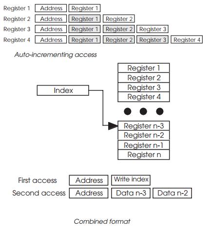
This is fine for small numbers of registers but with memory devices such
as EEPROM this is not an efficient method of opera-tion. An alternative method
uses an index value which is written to the chip, prior to accessing the data.
This is known as the combined format and uses two data transfers. The first
transfer is a write with the index value that is to be used to select the
location for the next access. To access memory byte 237, the data byte after
the address would contain 237. The next transfer would then send the data in
the case of a write or request the contents in the case of a read. Some devices
also support auto-incrementing and thus the second transfer can access multiple
sequential locations starting at the previously transmitted index value.
Timing
One of the more confusing points about the bus is the timing or lack of
it. The clock is not very specific about its timings and does not need a
specified frequency or even mark to space ratios. It can even be stopped and
restarted at a later point in time if needed. The START, STOP and ACKNOWLEDGE
signals have a minimum delay time between the clock and data edges and pulse
widths but apart from this, everything is very free and easy.
This is great in one respect but can cause problems in an other.
Typically the problem is concerned with waiting for the ACKNOWLEDGE signal
before proceeding. If this signal is not returned then the bus will be locked
up until the master terminates the transfers with a STOP signal. It is
important therefore not to miss the transition. Unfortunately, the time taken
for a slave to respond is dependent on the peripheral and with devices like
EEPROM, especially during a write cycle, this time can be ex-tremely long.
As a result, the master should use a timer/counter to determine when
sufficient time has been given to detect the ACKNOWLEDGE before issuing a STOP.
This can be done in several ways: polling can be used with a counter to
determine the timeout value. The polling loop is completed when either the
ACKNOWLEDGE is detected to give a success or if the polling count is exceeded.
An alternative method is to use a timer to tell the master when to check for
the acknowl-edgement. There are refinements that can be added where the timeout
values are changed depending on the peripheral that is being accessed. A very
sophisticated system can use a combina-tion of timer and polling to check for
the signal n times with an interval
determined by the timer. Whichever method is chosen, it is important that at
least one is implemented to ensure that the bus is not locked up.
Multi-master support
The bus supports the use of multiple masters but does not have any
in-built mechanism for controlling access. Instead, it uses a technique called
collision detect to determine if two masters start to use the bus at the same
time. A master waits until the bus is clear, i.e. there is no current transfer,
and then issues a START signal. If another master has done the same then the
signals that appear on the line will be corrupted. If a master wants a line to
be high and the other wants to drive it low, then the line will go low. With the
bidirectional ports that are used, each master can monitor the line and confirm
that it is in the expected state. If it is not, then a collision has occurred
and the master should discontinue trans-mission and allow the other master to
continue.
It is important that timeouts for acknowledgement are incorporated to
ensure that the bus cannot be locked up. In addition, care must be taken with
combined format accesses to prevent a second master from resetting the index on
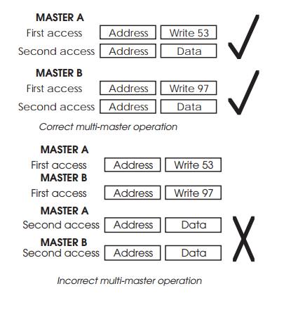
the periph-eral. If master A sets the index into an EEPROM peripheral to 53 and
before it starts the next START-address-data transfer, a sec-ond master gets
the bus and sets the index to its value of 97, the first master will access
incorrect data. The problem can be even worse as the diagram shows. When master
B overwrites the index value prior to master A’s second access, it causes data
corruption for both parties. Master A will access location 97 and due to
auto-incrementing, master B will access location 98 — neither of which is correct!
The bus does not provide a method of solving this dilemma and the only real
solutions are not to share the peripheral between the devices or use a
semaphore to protect access. The protection of resources is a perennial problem
with embedded systems and will be covered in more detail later on.
M-Bus (Motorola)
M-Bus is an ideal interface for EEPROMs, LCD controllers, A/D converters
and other components that could benefit from fast serial transfers. This
two-wire bidirectional serial bus allows a master and a slave to rapidly
exchange data. It allows for fast communication with no address translation. It
is very similar in operation to I2C and thus M-Bus devices can be used with these type of serial ports.
The maximum transfer rate is 100 kb/s.
Related Topics