Chapter: Embedded Systems Design : Basic peripherals
Serial peripheral interface
Serial peripheral interface
This bus is often referred to as the SPI and is frequently used on
Motorola processors such as the MC68HC05 and MC68HC11 microcontrollers to
provide a simple serial interface. It uses the basic interface as described in
the previous section with a shift register in the master and slave devices
driven by a common clock. It allows full-duplex synchronous communication
between the MCU and other slave devices such as peripherals and other
processors.
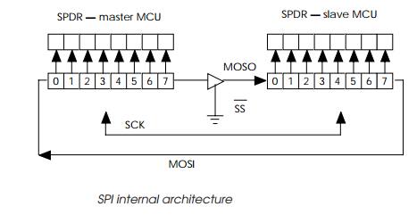
Data is written to the SPDR register in the master device and clocked
out into the slave device SPDR using the common clock signal SCK. When 8 bits
have been transferred, an interrupt is locally generated so that the data can
be read before the next byte is clocked through. The SS or slave select signal
is used to select which slave is to receive the data. In the first example,
shown with only one slave, this is permanently asserted by grounding the
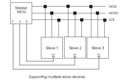
signal. With multiple slaves, spare parallel I/O pins are used to select the
slave prior to data transmission. The diagram below shows such a configuration.
If pin 1 on the master MCU is driven low, slave 1 is selected and so on. The
unselected slaves tri-state the SPI connections and do not receive the clocked
data and take no part in the transfer.
It should not be assumed that an implementation buffers data. As soon as
the master writes the data into the SPDR it is transmitted as there is no
buffering. As soon as the byte has been clocked out, an interrupt is generated
indicating that the byte has been transferred. In addition, the SPIF flag in the
status register (SPSR) is set. This flag must be cleared by the ISR before
transmit-ting the next byte.
The slave device does have some buffering and the data is transferred to
the SPDR when a complete byte is transferred. Again, an interrupt is generated
when a byte is received. It is essential that the interrupt that is generated
by the full shift register is serviced quickly to transfer the data before the
next byte is transmitted and transferred to the SPDR. This means that there is
an eight clock time period for the slave to receive the interrupt and transfer
the data. This effectively determines the maximum data rate.
Related Topics