Chapter: Electronic Devices : Power Devices and Display Devices
Power BJT(Power Bipolar Junction Transistor)
POWER BJT
Introduction
Bipolar Junction Transistor (BJT) is a three
terminal, three layer, two junction semiconductor device. Emitter(E), Base(B)
and Collector(C) are the three terminals of the device.
Symbol: The symbol of the Power BJT is
same as signal level transistor.
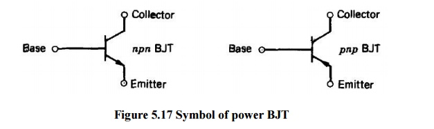
Figure 5.17 Symbol of power BJT
Structure
The construction of the Power Transistor is
different from the signal transistor as shown in the following figure. The n-
layer is added in the power BJT which is known as drift region.
·
A Power BJT has a four layer structure of
alternating P and N type doping as shown in above npn transistor.
·
It has three terminals labeled as Collector, Base,
Emitter.
·
In most of Power Electronic applications, the Power
Transistor works in Common Emitter configuration.
·
ie, Base is the input terminal, the Collector is
the output terminal and the Emitter is common between input and output.
·
In power switches npn transistors are most widely
used than pnp transistors.
·
The thickness of the dirft region determines the
breakdown voltage of the Power transistor.
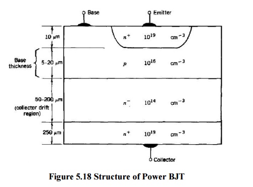
Figure 5.18 Structure of Power
BJT
·
The characteristics of the device is determined by
the doping level in each of the layers and the thickness of the layers.
VI Characteristics
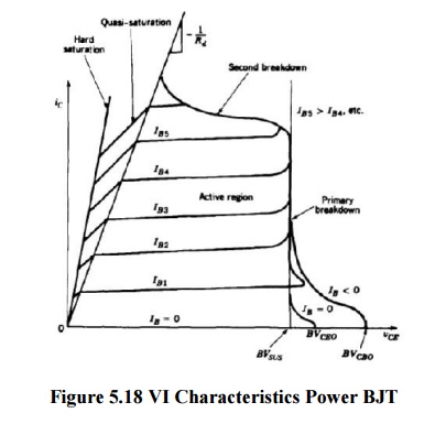
Figure 5.18 VI Characteristics
Power BJT
·
The VI
characteristics of the Power BJT is different from signal level transistor.
·
The major differences are Quasi saturation region
& secondary breakdown region.
·
The Quasi saturation region is available only in
Power transistor characteristic not in signal transistors. It is because of the
lightly doped collector drift region present in Power BJT.
·
The primary breakdown is similar to the signal
transistor's avalanche breakdown
·
Operation of device at primary and secondary
breakdown regions should be avoided as it will lead to the catastrophic failure
of the device.
Related Topics