Chapter: Electronic Devices : Power Devices and Display Devices
Photo Diode - Photo junction Devices
PHOTO JUNCTION DEVICES
Photo
junction Devices are basically PN-Junction light sensors or detectors made from
silicon semiconductor PN-junctions which are sensitive to light and which can
detect both visible light and infra-red light levels. Photo-junction devices
are specifically made for sensing light and this class of photoelectric light
sensors include the Photodiode and the Phototransistor.
PHOTODIODE
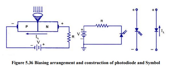
Symbol and construction of photo diode

Figure 5.36 Biasing arrangement
and construction of photodiode and Symbol
Photo-diode
is a two-terminal semiconductor P-N junction device and is designed to operate
with reverse bias. The basic biasing arrangement, construction and symbols for
the device are given in figure. It is either mounted in translucent case or has
its semiconductor junction mounted beneath an optical lens. The output voltage
is taken from across a series-connected load resistor R. This resistance may be
connected between the diode and ground or between the diode and the positive
terminal of the supply, as illustrated in figure.
When the
P-N junction is reverse-biased, a reverse saturation current flows due to
thermally generated holes and electrons being swept across the junction as the
minority carriers. With the increase in temperature of the junction more and
more hole-electron pairs are created and so the reverse saturation current I0
increases. The same effect can be had by illuminating the junction.
When
light energy bombards a P-N junction, it dislodges valence electrons. The more
light striking the junction the larger the reverse current in a diode. It is
due to generation of more and more charge carriers with the increase in level
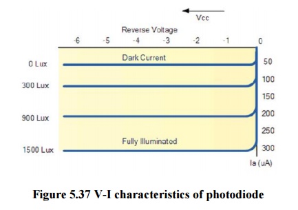
of illumination. This is clearly shown in figure 5.37 for different intensity
levels. The dark current is the
current that exists when no light is incident. It is to be noted here that
current becomes zero only with a positive applied bias equals to VQ.
The
almost equal spacing between the curves for the same increment in luminous flux
reveals that the reverse saturation current I0 increases linearly
with the luminous flux as shown in figure. Increase in reverse voltage does not
increase the reverse current significantly, because all available charge
carriers are already being swept across the junction. For reducing the reverse
saturation current I0 to zero, it is necessary to forward bias the
junction by an amount equal to barrier potential. Thus the photodiode can be
used as a photoconductive device.
V-I characteristics of photodiode

Figure 5.37 V-I characteristics
of photodiode
The
current-voltage characteristic (I/V Curves) of a photodiode with no light on
its junction (dark mode) is very similar to a normal signal or rectifying
diode. When the photodiode is forward biased, there is an exponential increase
in the current, the same as for a normal diode. When a reverse bias is applied,
a small reverse saturation current appears which causes an increase of the
depletion region, which is the sensitive part of the junction. Photodiodes can
also be connected in a current mode using a fixed bias voltage across the
junction. The current mode is very linear over a wide range.
On
removal of reverse bias applied across the photodiode, minority charge carriers
continue to be swept across the junction while the diode is illuminated. This
has the effect of increasing the concentration of holes in the P-side and that
of electrons in the N-side But the barrier potential is negative on the P-side
and positive on the N-side, and was created by holes flowing from P to N-side
and electrons from N to P-side during fabrication of junction. Thus the flow of
minority carriers tends to reduce the barrier potential.
When an
external circuit is connected across the diode terminals, the minority carrier;
return to the original side via the external circuit. The electrons which
crossed the junction from P to N-side now flow out through the N-terminal and
into the P-terminal This means that the device is behaving as a voltage cell
with the N-side being the negative terminal and the P-side the positive
terminal. Thus, the photodiode is & photovoltaic device as well as
photoconductive device.
When used
as a light sensor, a photodiodes dark current (0 lux) is about 10uA for
geranium and 1uA for silicon type diodes. When light fall upon the junction
more hole/electron pairs are formed and the leakage current increases. This
leakage current increases as the illumination of the junction increases. Thus,
the photodiodes current is directly proportional to light intensity falling
onto the PN-junction.
Advantage of photodiodes
One main
advantage of photodiodes when used as light sensors is their fast response to
changes in the light levels.
Disadvantage of photodiodes
One
disadvantage of this type of photo device is the relatively small current flow
even when fully lit.
Related Topics