Chapter: Electronic Devices : Power Devices and Display Devices
Double-Diffused MOS (DMOS)
DOUBLE-DIFFUSED MOS (DMOS)
The
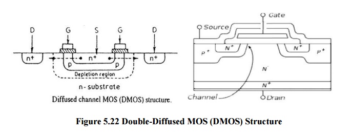
figure5.22 shows a double-diffused MOS (DMOS) structure. T he channel length,
L, is controlled by the junction de pth produced by the n+ and
p-type diffusions underneath the gate oxide. L is also the lateral distance
between the n+ p junction and the p-n substrate junction. The channel
length can be made to a smaller distance of about 0.5 micro meters. Thus, this
process is similar to the situation with resspect to the base width of a
double-diffused bipolar transistor. When a fairly large positive voltage is
applied to the gate [>VTH], it will cause the inversion of the
p-substrate region underneath thhe gate to n- type , and the n-type surface
inversion layer that is produced will act as a conducting channel for the flow
of electrons from sou rce to drain.

Figure 5.22 Double-Diffused MOS
(DMOS) Structure
From the
structure it is known that the n-type substrate is very lightly doped. This
will help in making enough space for thee expansion of the depletion region
between the p-type diffusion region and the n+ drain contact region.
Due to this, the breakdown voltage w ill become higher between the drain and
source.
Power MOSFET
The Power
MOSFET is the three terminal (Gate, Drain and Source), four layer (n+pnn+),Unipolar
( only majority carriers in conduction) semiconductor device.
Related Topics