Chapter: Electronic Devices : Power Devices and Display Devices
CCD( Charge Coupled Device)
CCD( CHARGE COUPLED DEVICE)
A charge-coupled device (CCD) is a device for the
movement of electrical charge, usually from within the device to an area where
the charge can be manipulated, for example conversion into a digital value.
This is achieved by "shifting" the signals between stages within the
device one at a time. CCDs move charge between capacitive bins in the device, with the shift allowing for the transfer of
charge between bins.
The CCD is a major piece of technology in digital
imaging. In a CCD image sensor, pixels are represented by p-doped MOS
capacitors. These capacitors are biased above the threshold for inversion when
image acquisition begins, allowing the conversion of incoming photons into
electron charges at the semiconductor-oxide interface; the CCD is then used to
read out these charges. Although CCDs are not the only technology to allow for
light detection, CCD image sensors are widely used in professional, medical,
and scientific applications where high-quality image data is required.
In
applications with less exacting quality demands, such as consumer and
professional digital cameras, active pixel sensors (CMOS) are generally used;
the large quality advantage CCDs enjoyed early on has narrowed over time.
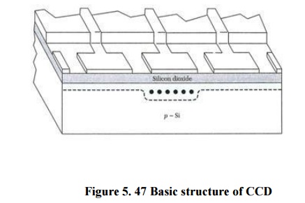
Figure 5.
47 Basic structure of CCD
In a CCD for
capturing images, there is a photoactive region (an epitaxial layer of
silicon), and a transmission region made out of a shift register (the CCD,
properly speaking).An image is projected through a lens onto the capacitor
array (the photoactive region), causing each capacitor to accumulate an
electric charge proportional to the light intensity at that location.
A one-
dimensional array, used in line-scan cameras, captures a single slice of the
image, while a two- dimensional array, used in video and still cameras,
captures a two-dimensional picture corresponding to the scene projected onto
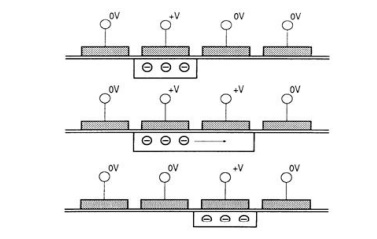
the focal plane of the sensor. Once the array has been exposed to the image, a
control circuit causes each capacitor to transfer its contents to its neighbor
(operating as a shift register).
The last
capacitor in the array dumps its charge into a charge amplifier, which converts
the charge into a voltage. By repeating this process, the controlling circuit
converts the entire contents of the array in the semiconductor to a sequence of
voltages. In a digital device, these voltages are then sampled, digitized, and
usually stored in memory; in an analog device (such as an analog video camera),
they are processed into a continuous analog signal (e.g. by feeding the output of
the charge amplifier into a low-pass filter) which is then processed and fed
out to other circuits for transmission, recording, or other processing.
Functional features
CCD can convert optical signals into digital signal
directly to achieve the acquisition, storage, transmission and proceeding of
images. The special characterizations are:
1. Small in
size and light in weight.
2. Low power
consumption, low working voltage.
3. Stable
performance and long operational life, resistant of impact and vibration
4. High
sensitivity, low noise and large dynamic range
5. Quick
respond, with self-scanning function, small image distortion, non-residual
image
6. Applicable
to ultra-large scale integrated circuit, with high integration of pixel,
accurate size, and low cost
Applications of CCD
Consequently,
CCD shows wide applications in varied fields.
CCD device and its application technology have been
developed, and remarkable progress, especially in the mage sensor and
non-contact measurement have been made in the past decades years. With the
theory development, CCD becomes a high-sensitivity device and used in many
regions. Some of them are listed here in this report:
1 CCD digital camera
CCD cameras contain light-sensitive silicon chips
that detect electrons excited by incoming light, and the micro circuitry that
transfers a detected signal along a row of discrete picture elements or pixels,
scanning the image very rapidly [9]. Two-dimensional CCD arrays with
many thousands of pixels are used in these CCD cameras, and they are often used
in machine vision applications.
CCD
cameras can operate in both monochrome (black, white, and grayscale) and color.
The range of colors is generated by varying combinations of different discrete
colors, like red, green, and blue components (RGB), to create a wide spectrum
of colors. Important performances of CCD cameras include horizontal resolution,
maximum frame rate, shutter speed, sensitivity, and signal-to-noise ratio.
Other parameters to consider when specifying CCD cameras include specialty
applications, performance features, physical features, lens mounting, shutter
control, sensor specifications, dimensions, and operating environment
parameters.
The CCD camera can be applied in astronomy,
medicine, optical scanner, etc., as its high quantum efficiencies, linearity of
outputs and ease of use.
2 CCD image sensor
CCD image
sensors are electronic devices which are capable of transforming a light
pattern (image) into an electric charge pattern (an electronic image). The CCD
consists of several individual elements that have the capability of collecting,
storing and transporting electrical charge from one element to another, as
described in the theory part. Together with the photosensitive properties of
silicon, CCD is used to design image sensors.
With semiconductor technologies and design rules,
one or more output amplifiers at the edge of the chip collect the signals from
the CCD, and electronic images can be obtained by applying series of pulses
that transfer the charge of one pixel after another to the output amplifier,
line after line. The output amplifier converts the charge into a voltage, while
external electronics will transform this output signal into a form suitable for
monitors or frame grabbers. Thus CCDs have extremely low noise figures.CCD
image sensors can also be a color sensor or a monochrome sensor, as the CCD
camera.
Important image sensor performances include
spectral response, data rate, quantum efficiency, dynamic range, and number of
outputs. An important environmental parameter to consider is the operating
temperature.
CCD image sensors have found important applications
in many areas of society and science, like digital cameras, scanners, medical
devices, satellite surveillance and in instrumentation for astronomy and
astrophysics.
3Optical scanner
CCD used
in fax machines forms images on the surface of arrayed capacitor. The
brightness of images produces each capacity with charges, which can be
transferred to amplifier and forms voltage at the edge of circuit. With the
information of the voltage, the images can be stored and print out.
Related Topics