Chapter: Microprocessor and Microcontroller
I/O Port Configuration in 8051
I/O Port Configuration
Each port
of 8051 has bidirectional capability. Port 0 is called 'true bidirectional
port' as it floats (tristated) when configured as input. Port-1, 2, 3 are
called 'quasi bidirectional port'. Port-0 Pin Structure
Port -0
has 8 pins (P0.0-P0.7).
The
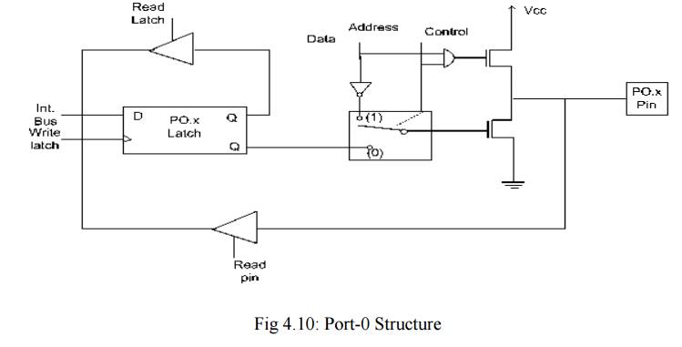
structure of a Port-0 pin is shown in fig 4.10.
Port-0
can be configured as a normal bidirectional I/O port or it can be used for
address/data interfacing for accessing external memory. When control is '1',
the port is used for address/data interfacing. When the control is '0', the
port can be used as a normal bidirectional I/O port.
Let us
assume that control is '0'. When the port is used as an input port, '1' is
written to the latch. In this situation both the output MOSFETs are 'off'.
Hence the output pin floats. This high impedance pin can be pulled up or low by
an external source. When the port is used as an output port, a '1' written to
the latch again turns 'off' both the output MOSFETs and causes the output pin
to float. An external pull-up is required to output a '1'. But when '0' is
written to the latch, the pin is pulled down by the lower MOSFET. Hence the
output becomes zero.
When the
control is '1', address/data bus controls the output driver MOSFETs. If the
address/data bus (internal) is '0', the upper MOSFET is 'off' and the lower
MOSFET is 'on'. The output becomes '0'. If the address/data bus is '1', the
upper transistor is 'on' and the lower transistor is 'off'. Hence the output is
'1'. Hence for normal address/data interfacing (for external memory access) no
pull-up resistors are required.
Port-0
latch is written to with 1's when used for external memory access. Port-1 Pin
Structure
Port-1
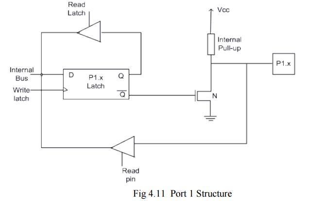
has 8 pins (P1.1-P1.7) .The structure of a port-1 pin is shown in fig 4.11.
Port-1
does not have any alternate function i.e. it is dedicated solely for I/O
interfacing. When used as output port, the pin is pulled up or down through
internal pull-up. To use port-1 as input port, '1' has to be written to the
latch. In this input mode when '1' is written to the pin by the external device
then it read fine. But when '0' is written to the pin by the external device
then the external source must sink current due to internal pull-up. If the
external device is not able to sink the current the pin voltage may rise,
leading to a possible wrong reading.
PORT 2
Pin Structure
Port-2
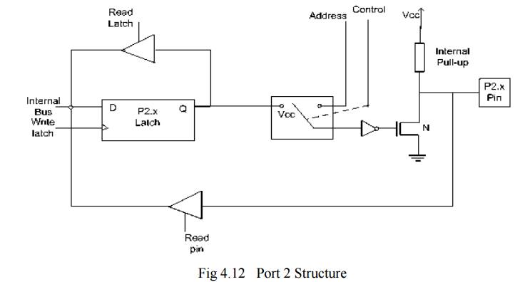
has 8-pins (P2.0-P2.7) . The structure of a port-2 pin is shown in fig 4.12.
Port-2 is
used for higher external address byte or a normal input/output port. The I/O
operation is similar to Port-1. Port-2 latch remains stable when Port-2 pin are
used for external memory access. Here again due to internal pull-up there is
limited current driving capability.
PORT 3
Pin Structure
Port-3
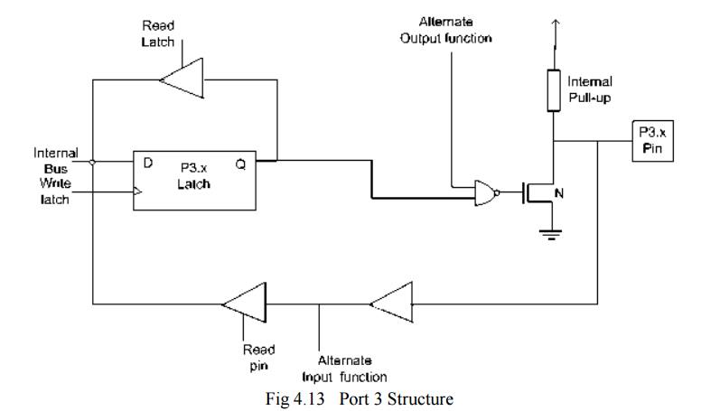
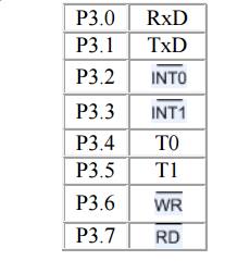
has 8 pin (P3.0-P3.7) . Port-3 pins have alternate functions. The structure of
a port-3 pin is shown in fig 4.13.
Each pin
of Port-3 can be individually programmed for I/O operation or for alternate
function. The alternate function can be activated only if the corresponding
latch has been written to '1'. To use the port as input port, '1' should be
written to the latch. This port also has internal pull-up and limited current
driving capability.
Alternate
functions of Port-3 pins are –
Note:
1. Port 1,
2, 3 each can drive 4 LS TTL inputs.
2. Port-0
can drive 8 LS TTL inputs in address /data mode. For digital output port, it
needs external pull-up resistors.
3. Ports-1,2and
3 pins can also be driven by open-collector or open-drain outputs.
4. Each Port
3 bit can be configured either as a normal I/O or as a special function bit.
There is
a subtle difference between reading a latch and reading the output port pin.
The
status of the output port pin is sometimes dependant on the connected load. For
instance if a port is configured as an output port and a '1' is written to the
latch, the output pin should also show '1'. If the output is used to drive the
base of a transistor, the transistor turns 'on'.
If the port
pin is read, the value will be '0' which is corresponding to the base-emitter
voltage of the transistor.
Reading a latch: Usually the instructions that
read the latch, read a value, possibly change it, and then rewrite it to the latch. These are called
"read-modify-write" instructions. Examples of a few instructions are-
ORL P2,
A; P2 <-- P2 or A
MOV P2.1,
C; Move carry bit to PX.Y bit.
In this
the latch value of P2 is read, is modified such that P2.1 is the same as Carry
and is then written back to P2 latch.
Reading a Pin: Examples of a few instructions
that read port pin, are-
MOV A, P0
; Move port-0 pin values to A
MOV A,
P1; Move port-1 pin values to A
Accessing
external memory

P3.7 and
P3.6).
For
external program memory, always 16 bit address is used. For example - MOVC A, @
A+DPTR
MOVC A, @
A+PC
Access to
external data memory can be either 8-bit address or 16-bit address - 8-bit
address- MOVX A, @Rp where Rp is either R0 or R1
MOVX @Rp,
A
16 bit
address- MOVX A,@DPTR
MOV X
@DPTR, A
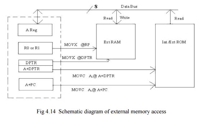
The
external memory access in 8051 can be shown by a schematic diagram as given in
fig 4.14.
If an
8-bit external address is used for data memory (i.e. MOVX @Rp) then the content
of Port-2 SFR remains at Port-2 pins throughout the external memory cycle. This
facilitates memory paging as the upper 8 bit address remains fixed.
During
any access to external memory, the CPU writes FFH to Port-0 latch (SFR). If the
user writes to Port-0 during an external memory fetch, the incoming byte is
corrupted. External program memory is accessed under the following condition.

Some
typical use of code/program memory access:
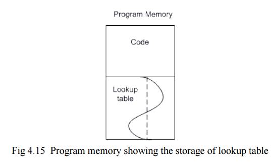
External
program memory can be not only used to store the code, but also for lookup
table of various functions required for a particular application. Mathematical
functions such as Sine, Square root, Exponential, etc. can be stored in the
program memory (Internal or eternal) and these functions can be accessed using
MOVC instruction.
Timers /
Counters
8051 has
two 16-bit programmable UP timers/counters. They can be configured to operate
either as timers or as event counters. The names of the two counters are T0 and
T1 respectively. The timer content is available in four 8-bit special function
registers, viz, TL0,TH0,TL1 and TH1 respectively.
In the
"timer" function mode, the counter is incremented in every machine
cycle. Thus, one can think of it as counting machine cycles. Hence the clock
rate is 1/12 th of the oscillator frequency.
In the
"counter" function mode, the register is incremented in response to a
1 to 0 transition at its corresponding external input pin (T0 or T1). It
requires 2 machine cycles to detect a high to low transition. Hence maximum
count rate is 1/24 th of oscillator frequency.
The
operation of the timers/counters is controlled by two special function
registers, TMOD and TCON respectively.
Timer
Mode control (TMOD) Special Function Register:
TMOD
register is not bit addressable.
TMOD
Address:
89 H
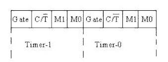
Various
bits of TMOD are described as follows -
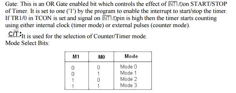
M1 and M0
are mode select bits.
Timer/
Counter control logic:
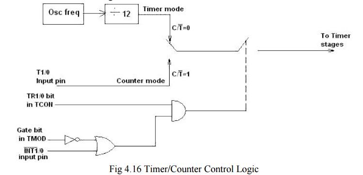
Fig 4.16
Timer/Counter Control Logic Timer control (TCON) Special function register:
TCON is
bit addressable. The address of TCON is 88H. It is partly related to Timer and
partly to interrupt.
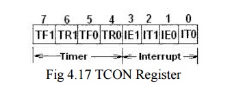
The
various bits of TCON are as follows.
TF1 :
Timer1 overflow flag. It is set when timer rolls from all 1s to 0s. It is
cleared when processor vectors to execute ISR located at address 001BH.
TR1 :
Timer1 run control bit. Set to 1 to start the timer / counter. TF0 : Timer0
overflow flag. (Similar to TF1)
TR0 : Timer0
run control bit.
IE1 :
Interrupt1 edge flag. Set by hardware when an external interrupt edge is
detected. It is cleared when interrupt is processed.
IE0 :
Interrupt0 edge flag. (Similar to IE1)
IT1 :
Interrupt1 type control bit. Set/ cleared by software to specify falling edge /
low level triggered external interrupt.
IT0 :
Interrupt0 type control bit. (Similar to IT1)
As
mentioned earlier, Timers can operate in four different modes. They are as
follows Timer Mode-0:
In this
mode, the timer is used as a 13-bit UP counter as follows.
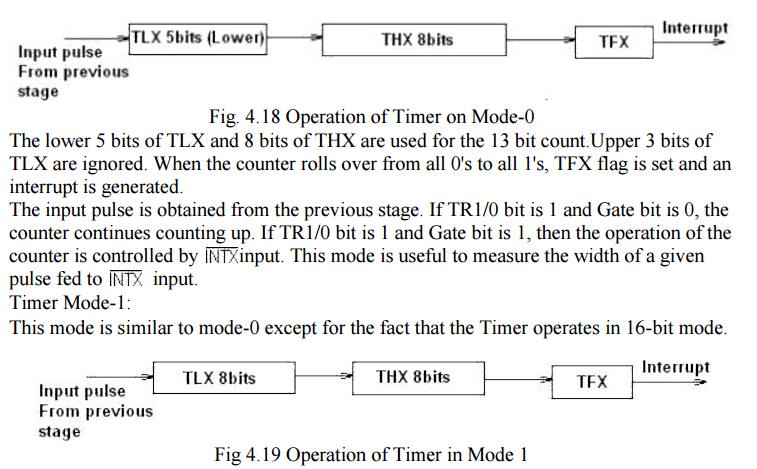
Timer
Mode-2: (Auto-Reload Mode)
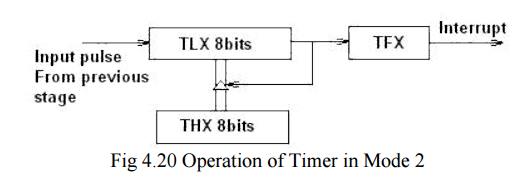
This is a
8 bit counter/timer operation. Counting is performed in TLX while THX stores a
constant value. In this mode when the timer overflows i.e. TLX becomes FFH, it
is fed with the value stored in THX. For example if we load THX with 50H then
the timer in mode 2 will count from 50H to FFH. After that 50H is again
reloaded. This mode is useful in applications like fixed time sampling.
Timer
Mode-3:
Timer 1
in mode-3 simply holds its count. The effect is same as setting TR1=0. Timer0
in mode-3 establishes TL0 and TH0 as two separate counters.
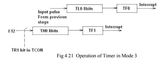
Control
bits TR1 and TF1 are used by Timer-0 (higher 8 bits) (TH0) in Mode-3 while TR0
and TF0 are available to Timer-0 lower 8 bits(TL0).
Related Topics