Chapter: Microprocessor and Microcontroller : Peripheral Interfacing
Programmable Keyboard/Display Interface- 8279
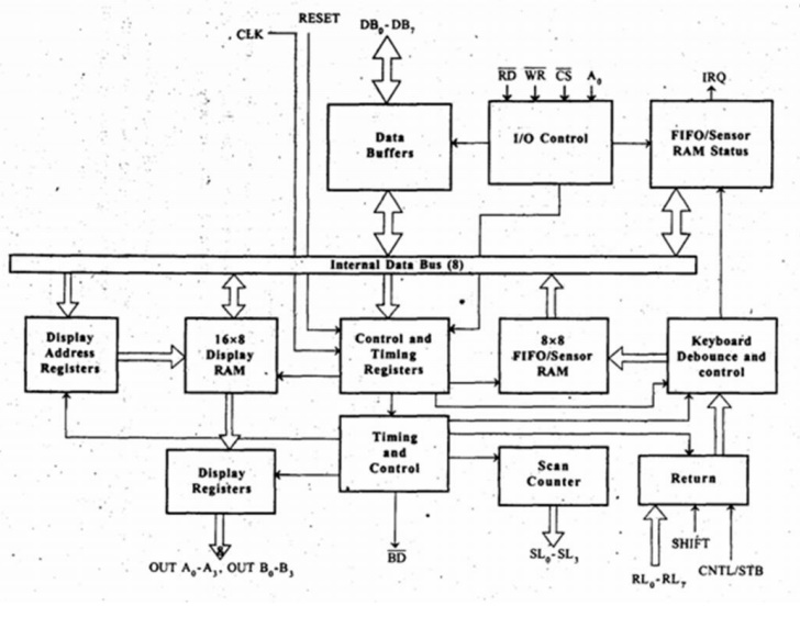
Programmable Keyboard/Display Interface - 8279
A programmable keyboard and display interfacing chip. Scans and encodes up to a 64-key keyboard. Controls up to a 16-digit numerical display. Keyboard section has a built-in FIFO 8 character buffer. The display is controlled from an internal 16x8 RAM that stores the coded display information.
1 Pinout Definition 8279
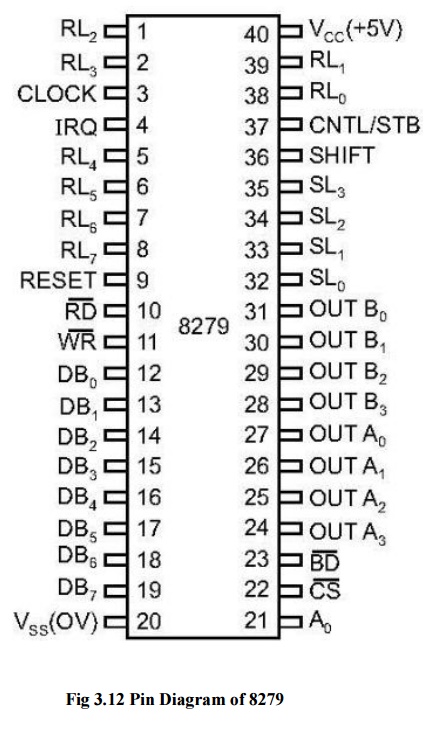
ü A0: Selects data (0) or control/status (1) for reads and writes between micro and 8279.
ü BD: Output that blanks the displays.
ü CLK: Used internally for timing. Max is 3 MHz.
ü CN/ST: Control/strobe, connected to the control key on the keyboard
ü CS: Chip select that enables programming, reading the keyboard, etc.
ü DB7-DB0: Consists of bidirectional pins that connect to data bus on micro.
ü IRQ: Interrupt request, becomes 1 when a key is pressed, data is available.
ü OUT A3-A0/B3-B0: Outputs that sends data to the most significant/least significant nibble of display.
ü RD(WR): Connects to micro's IORC or RD signal, reads data/status registers.
ü RESET: Connects to system RESET.
ü RL7-RL0: Return lines are inputs used to sense key depression in the keyboard matrix.
ü Shift: Shift connects to Shift key on keyboard.
ü SL3-SL0: Scan line outputs scan both the keyboard and displays.
2 Block Diagram of 8279
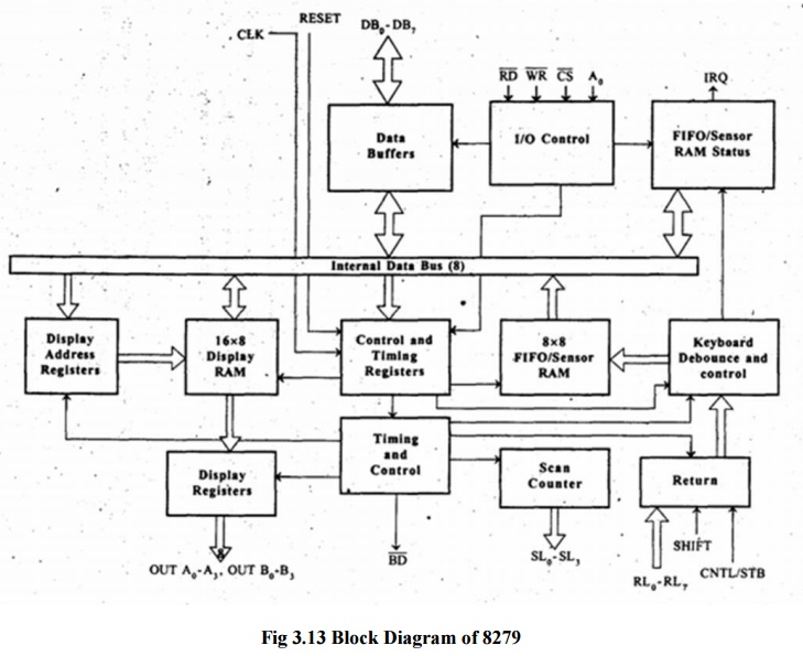
Display section:
ü The display section has eight output lines divided into two groups A0-A3 and B0-B3.
ü The output lines can be used either as a single group of eight lines or as two groups of four lines, in conjunction with the scan lines for a multiplexed display.
ü The output lines are connected to the anodes through driver transistor in case of common cathode 7-segment LEDs.
ü The cathodes are connected to scan lines through driver transistors.
ü The display can be blanked by BD (low) line.
ü The display section consists of 16 x 8 display RAM. The CPU can read from or write into any location of the display RAM.
Scan section:
ü The scan section has a scan counter and four scan lines, SL0 to SL3.
ü In decoded scan mode, the output of scan lines will be similar to a 2-to-4 decoder.
ü In encoded scan mode, the output of scan lines will be binary count, and so an external decoder should be used to convert the binary count to decoded output.
ü The scan lines are common for keyboard and display.
ü The scan lines are used to form the rows of a matrix keyboard and also connected to digit drivers of a multiplexed display, to turn ON/OFF.
CPU interface section:
ü The CPU interface section takes care of data transfer between 8279 and the processor.
ü This section has eight bidirectional data lines DB0 to DB7 for data transfer between 8279 and CPU. It requires two internal address A =0 for selecting data buffer and A = 1 for selecting control register of8279.
ü The control signals WR (low), RD (low), CS (low) and A0 are used for read/write to 8279.
ü It has an interrupt request line IRQ, for interrupt driven data transfer with processor.
ü The 8279 require an internal clock frequency of 100 kHz. This can be obtained by dividing the input clock by an internal prescaler.
ü The RESET signal sets the 8279 in 16-character display with two -key lockout keyboard modes.
3 Keyboard Interface of 8279
The keyboard matrix can be any size from 2x2 to 8x8.Pins SL2-SL0 sequentially scan each column through a counting operation. The 74LS138 drives 0's on one line at a time. The 8279 scans RL pins synchronously with the scan. RL pins incorporate internal pull-ups, no need for external resistor pull-ups. The 8279 must be programmed first.
First three bits given below select one of 8 control registers (opcode).
000DDMMM
Mode set: Opcode 000.
DD sets displays mode.
MMM sets keyboard mode.
DD field selects either:
ü 8- or 16-digit display
ü Whether new data are entered to the rightmost or leftmost display position.
MMM Field:
DD Function
000 Encoded keyboard with 2 key lockout
001 Decoded keyboard with 2 key lockout
010 Encoded keyboard with N key rollover
011 Decoded keyboard with N key rollover
100 Encoded sensor matrix
101 Decoded sensor matrix
110 Strobed keyboard, encoded display scan
111 Strobed keyboard, decoded display scan
Encoded: SL outputs are active-high, follow binary bit pattern 0-7 or 0-15.
Decoded: SL outputs are active-low (only one low at any time).
Pattern output: 1110, 1101, 1011, 0111.
Strobed: An active high pulse on the CN/ST input pin strobes data from the RL pins into an internal FIFO for reading by micro later.
2-key lockout/N-key rollover: Prevents 2 keys from being recognized if pressed simultaneously/Accepts all keys pressed from 1st to last.
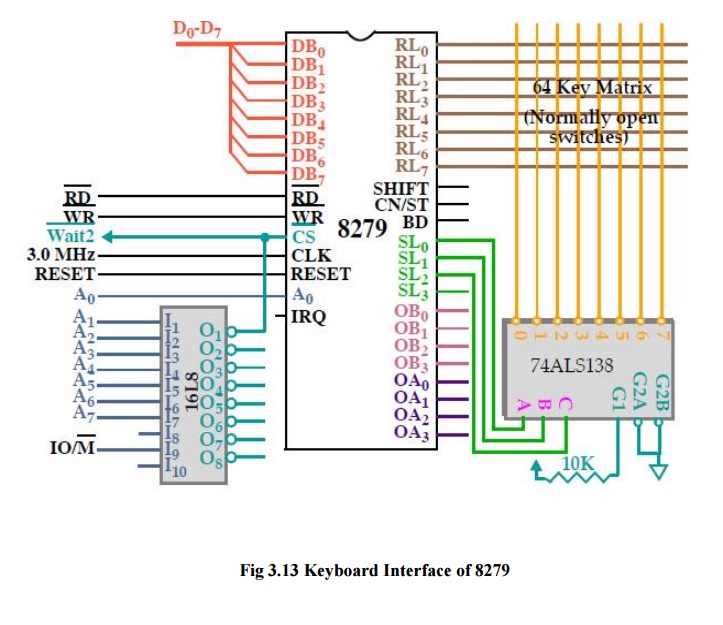
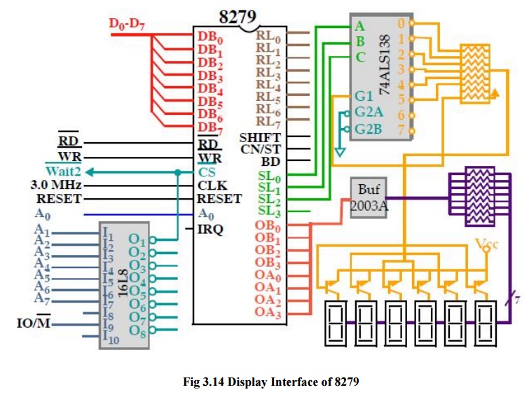
Fig 3.14 Display Interface of 8279
Related Topics