Chapter: Microprocessor and Microcontroller : Peripheral Interfacing
Programmable peripheral interface (8255): Architecture, Pin Diagram, Operational Modes and Control Word Format
Programmable peripheral interface
(8255)
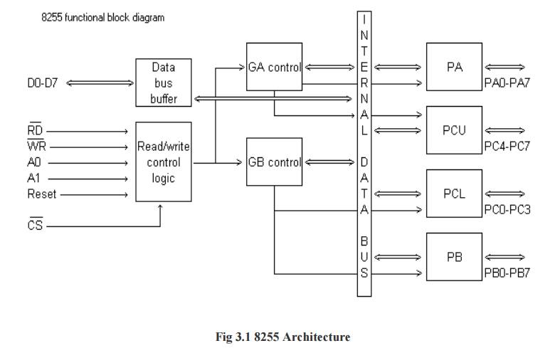
1 Architecture of 8255
The
parallel input-output port chip 8255 is also called as programmable peripheral
input- output port. The Intel’s 8255 is designed for use with Intel’s 8-bit,
16-bit and higher capability microprocessors.
It has 24
input/output lines which may be individually programmed in two groups of twelve
lines each, or three groups of eight lines. The two groups of I/O pins are
named as Group A and Group B. Each of these two groups contains a subgroup of
eight I/O lines called as 8-bit port and another subgroup of four lines or a
4-bit port.
Thus
Group A contains an 8-bit port A along with a 4-bit port. C upper. The port A
lines are identified by symbols PA0-PA7 while the port C lines are identified
as PC4-PC7. Similarly, Group B contains an 8-bit port B, containing lines
PB0-PB7 and a 4-bit port C with lower bits PC0- PC3. The port C upper and port
C lower can be used in combination as an 8-bit port C. Both the port C are
assigned the same address. Thus one may have either three 8-bit I/O ports or
two 8-bit and two 4-bit ports from 8255. All of these ports can function
independently either as input or as output ports. This can be achieved by programming
the bits of an internal register of 8255 called as control word register (CWR).
This buffer receives or transmits data upon the execution of input or output
instructions by the microprocessor. The control words or status information is
also transferred through the buffer.
2 Pin Diagram of 8255
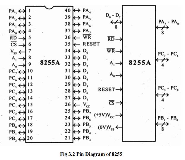
The
signal description of 8255 are briefly presented as follows:
ü PA7-PA0: These are eight port A lines
that acts as either latched output or buffered input lines depending upon the control word loaded into the control word
register.
ü PC7-PC4: Upper nibble of port C lines.
They may act as either output latches or input buffers lines. This port also can be used for
generation of handshake lines in mode 1 or mode 2.
ü PC3-PC0: These are the lower port C
lines, other details are the same as PC7-PC4 lines.
ü PB0-PB7: These are the eight port B
lines which are used as latched output lines or buffered input lines in the same way as port A.
ü RD: This is the input line driven
by the microprocessor and should be low to indicate read operation to 8255.
ü WR: This is an input line driven by
the microprocessor. A low on this line indicates write operation.
ü CS: This is a chip select line. If
this line goes low, it enables the 8255 to respond to RD and WR signals, otherwise RD and WR signal
are neglected.
ü A1-A0: These are the address input
lines and are driven by the microprocessor. These lines A1-A0 with RD, WR and CS from the following
operations for 8255. These address lines are used for addressing any one of the
four registers, i.e. three ports and a control word register as given in table
below. In case of 8086 systems, if the 8255 is to be interfaced with lower
order data bus, the A0 and A1 pins of 8255 are connected with A1 and A2
respectively.
ü D0-D7: These are the data bus lines
those carry data or control word to/from the microprocessor.
ü RESET: A logic high on this line
clears the control word register of 8255. All ports are set as input ports by default after reset.
3 Operational Modes of 8255
There are
two main operational modes of 8255:
ü Input/output
mode
ü Bit
set/reset mode
1 Input / Output Mode
There are
three types of the input/output mode. They are as follows:
Mode 0
In this
mode, the ports can be used for simple input/output operations without
handshaking. If both port A and B are initialized in mode 0, the two halves of
port C can be either used together as an additional 8-bit port, or they can be
used as individual 4-bit ports. Since the two halves of port C are independent,
they may be used such that one-half is initialized as an input port while the
other half is initialized as an output port. The input output features in mode
0 are as follows:
ü O/p are
latched.
ü I/p are
buffered not latched.
ü Port do
not have handshake or interrupt capability.
Mode 1
When we
wish to use port A or port B for handshake (strobed) input or output operation,
we initialize that port in mode 1 (port A and port B can be initialized to
operate in different modes, ie, for eg., port A can operate in mode 0 and port
B in mode 1). Some of the pins of port C function as handshake lines.
For port
B in this mode (irrespective of whether is acting as an input port or output
port), PC0, PC1 and PC2 pins function as handshake lines. If port A is
initialized as mode 1 input port, then, PC3, PC4 and PC5 function as handshake
signals. Pins PC6 and PC7 are available for use as input/output lines. The mode
1 which supports handshaking has following features: 1.
Two ports
i.e. port A and B can be used as 8-bit I/O port. 2. Each port uses three lines
of port c as handshake signal and remaining two signals can be function as I/O
port. 3. Interrupt logic is supported. 4. Input and Output data are latched.
Mode 2
Only
group A can be initialized in this mode. Port A can be used for bidirectional
handshake data transfer. This means that data can be input or output on the
same eight lines (PA0 - PA7). Pins PC3 - PC7 are used as handshake lines for
port A. The remaining pins of port C (PC0 - PC2) can be used as input/output
lines if group B is initialized in mode 0. In this mode, the 8255 may be used
to extend the system bus to a slave microprocessor or to transfer data bytes to
and from a floppy disk controller.
2 Bit Set/Reset (BSR) mode
In this
mode only port b can be used (as an output port). Each line of port C (PC0 -
PC7) can be set/reset by suitably loading the command word register.no effect
occurs in input-output mode. The individual bits of port c can be set or reset
by sending the signal OUT instruction to the control register.
4 Control Word Format
1 Input/output mode format
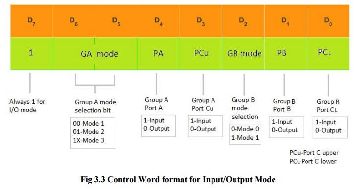
ü The
figure shows the control word format in the input/output mode. This mode is
selected by making
D7 = '1' .
ü D0, D1, D3, D4 are for lower port C, port B,
upper port C and port A respectively. When D0 or D1 or D3 or D4 are "SET", the corresponding ports act as
input ports. For eg, if D0 = D4 = '1', then lower port C and port A act as
input ports. If these bits are "RESET", then the corresponding ports
act as output ports. For eg, if D1 = D3 = '0', then port B and upper port C act
as output ports.
ü D2 is used for mode selection for
group B (Port B and Lower Port C). When D2 = '0', mode 0 is selected and when D2 = '1', mode 1 is selected.
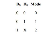
ü D5, D6 are used for mode selection for
group A (Upper Port C and Port A). The format is as follows:
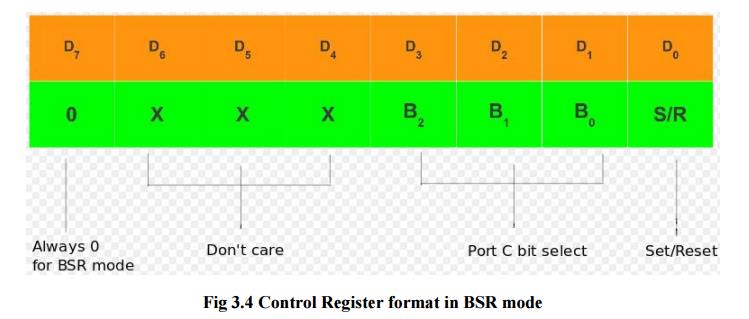
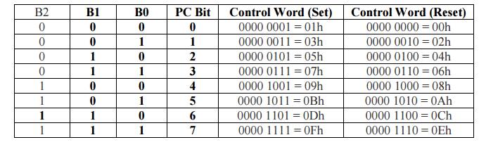
2 BSR mode format
ü Control
Word format in BSR mode
ü The
figure shows the control word format in BSR mode. This mode is selected by
making
D7='0'.
ü D0 is used for bit set/reset. When
D0= '1', the port C bit selected (selection of a port C bit is shown in the next point) is SET, when D0 = '0', the port C bit is RESET.
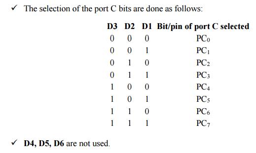
ü D1, D2, D3 are used to select a particular
port C bit whose value may be altered using D0 bit as mentioned above.
Related Topics