Chapter: Microprocessor and Microcontroller : 8085 Microprocessor
Timing Diagram and machine cycles of 8085 Microprocessor
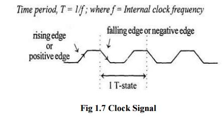
Timing Diagram
Timing Diagram is a graphical representation. It represents the
execution time taken by each instruction in a graphical format. The execution
time is represented in T-states.
Instruction Cycle:
The time
required to execute an instruction is called instruction cycle.
Machine Cycle:
The time
required to access the memory or input/output devices is called machine cycle.
T-State:
ü The
machine cycle and instruction cycle takes multiple clock periods.
ü A portion
of an operation carried out in one system clock period is called as T-state.
1 Machine cycles of 8085
The 8085
microprocessor has 5 (seven) basic machine cycles. They are
ü Opcode
fetch cycle (4T)
ü Memory
read cycle (3 T)
ü Memory
write cycle (3 T)
ü I/O read
cycle (3 T)
ü I/O write
cycle (3 T)
Signal 1.Opcode fetch machine cycle of 8085 :
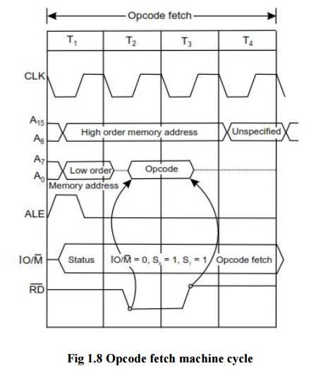
ü Each
instruction of the processor has one byte opcode.
ü The
opcodes are stored in memory. So, the processor executes the opcode fetch
machine cycle to fetch the opcode from memory.
ü Hence,
every instruction starts with opcode fetch machine cycle.
ü The time
taken by the processor to execute the opcode fetch cycle is 4T.
ü In this
time, the first, 3 T-states are used for fetching the opcode from memory and
the remaining T-states are used for internal operations by the processor.
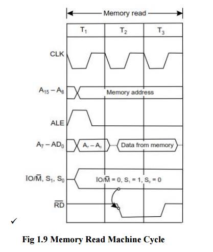
2. Memory Read Machine Cycle of 8085:
ü The
memory read machine cycle is executed by the processor to read a data byte from
memory.
ü The
processor takes 3T states to execute this cycle.
The
instructions which have more than one byte word size will use the machine cycle
after the opcode fetch machine cycle.
Cycle 3. Memory Write Machine Cycle of 8085
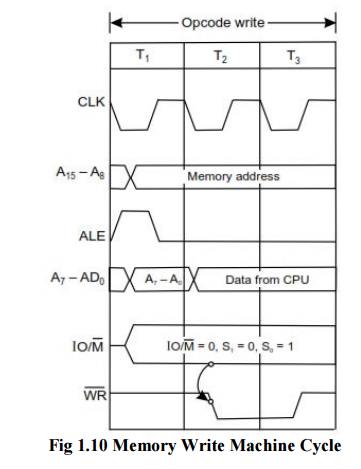
ü The
memory write machine cycle is executed by the processor to write a data byte in
a memory location.
ü The
processor takes, 3T states to execute this machine cycle.
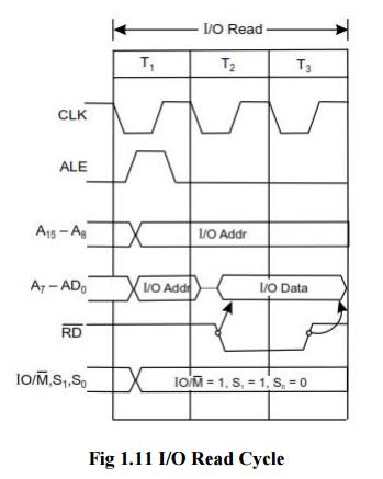
4. I/O Read Cycle of 8085
ü The I/O
Read cycle is executed by the processor to read a data byte from I/O port or
from the peripheral, which is I/O, mapped in the system.
ü The
processor takes 3T states to execute this machine cycle.
ü The IN
instruction uses this machine cycle during the execution.
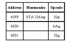
Cycle 1.4.2 Timing diagram for STA 526AH
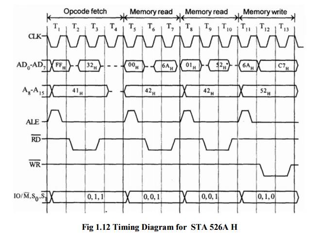
ü STA means
Store Accumulator -The contents of the accumulator is stored in the specified
address (526A).
ü The
opcode of the STA instruction is said to be 32H. It is fetched from the memory
41FFH (see fig). - OF machine cycle
ü Then the
lower order memory address is read (6A). - Memory Read Machine Cycle
ü Read the
higher order memory address (52).- Memory Read Machine Cycle
ü The
combination of both the addresses are considered and the content from
accumulator is written in 526A. - Memory Write Machine Cycle
ü Assume
the memory address for the instruction and let the content of accumulator is
C7H. So, C7H from accumulator is now stored in 526A.
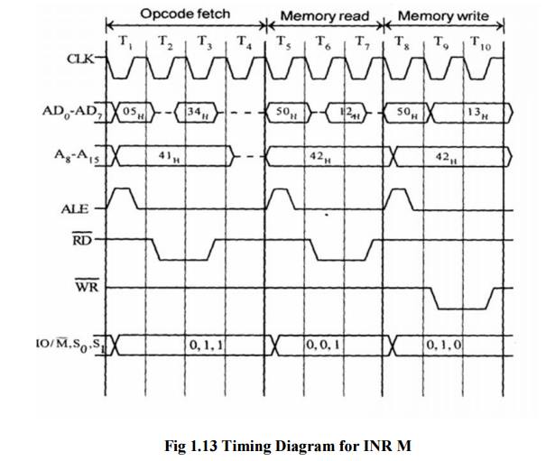
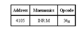
3 Timing diagram for INR M
ü Fetching
the Opcode 34H from the memory 4105H. (OF cycle)
ü Let the
memory address (M) be 4250H. (MR cycle -To read Memory address and data)
ü Let the
content of that memory is 12H.
ü Increment
the memory content from 12H to 13H. (MW machine cycle)
Related Topics