Chapter: Microprocessor and Microcontroller : 8085 Microprocessor
Hardware Architecture of 8085 Microprocessor
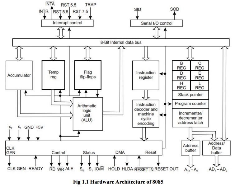
Hardware Architecture of 8085
Microprocessor
Control Unit:
Generates
signals within Microprocessor to carry out the instruction, which has been
decoded. In reality causes certain connections between blocks of the µP to be
opened or closed, so that data goes where it is required, and so that ALU
operations occur.
Arithmetic Logic Unit:
The ALU
performs the actual numerical and logic operation such as add, subtract, AND,
OR, etc. Uses data from memory and from Accumulator to perform arithmetic.
Always stores result of operation in Accumulator.
Registers:
The
8085/8080A-programming model includes six registers, one accumulator, and one
flag register, as shown in Figure. In addition, it has two 16-bit registers:
the stack pointer and the program counter. The 8085/8080A has six
general-purpose registers to store 8-bit data; these are identified as B, C, D,
E, H, and L as shown in the figure. They can be combined as register pairs -
BC, DE, and HL - to perform some 16-bit operations. The programmer can use
these registers to store or copy data into the registers by using data copy
instructions.
Accumulator:
The
accumulator is an 8-bit register that is a part of arithmetic/logic unit (ALU).
This register is used to store 8-bit data and to perform arithmetic and logical
operations. The result of an operation is stored in the accumulator. The
accumulator is also identified as register A.
Flags:
The ALU
includes five flip-flops, which are set or reset after an operation according
to data conditions of the result in the accumulator and other registers. They
are called Zero (Z), Carry (CY), Sign (S), Parity (P), and Auxiliary Carry (AC)
flags. The most commonly used flags are Zero, Carry, and Sign. The microprocessor
uses these flags to test data conditions.
For
example, after an addition of two numbers, if the sum in the accumulator id
larger than eight bits, the flip-flop uses to indicate a carry -- called the
Carry flag (CY) – is set to one. When an arithmetic operation results in zero,
the flip-flop called the Zero (Z) flag is set to one. The first Figure shows an
8-bit register, called the flag register, adjacent to the accumulator. However,
it is not used as a register; five bit positions out of eight are used to store
the outputs of the five flip-flops. The flags are stored in the 8-bit register
so that the programmer can examine these flags (data conditions) by accessing
the register through an instruction.
These
flags have critical importance in the decision-making process of the
microprocessor. The conditions (set or reset) of the flags are tested through
the software instructions. For example, the instruction JC (Jump on Carry) is
implemented to change the sequence of a program when CY flag is set.
Program Counter (PC):
This
16-bit register deals with sequencing the execution of instructions. This
register is a memory pointer. Memory locations have 16-bit addresses, and that
is why this is a16-bit register. The microprocessor uses this register to sequence
the execution of the instructions. The function of the program counter is to
point to the memory address from which the next byte is to be fetched. When a
byte (machine code) is being fetched, the program counter is incremented by one
to point to the next memory location
Stack Pointer (SP):
The stack
pointer is also a 16-bit register used as a memory pointer. It points to a
memory location in R/W memory, called the stack. The beginning of the stack is
defined by loading 16- bit address in the stack pointer.
Instruction Register/Decoder:
Temporary
store for the current instruction of a program. Latest instruction sent here
from memory prior to execution. Decoder then takes instruction and „decodes‟ or
interprets the instruction. Decoded instruction then passed to next stage.
Memory Address Register:
Holds
address, received from PC, of next program instruction. Feeds the address bus
with addresses of location of the program under execution.
Control Generator:
Generates
signals within µ P to carry out the instruction which has been decoded.
In
reality causes certain connections between blocks of the µP to be opened or
closed, so that data goes where it is required, and so that ALU operations
occur.
Register Selector:
This
block controls the use of the register stack in the example. Just a logic
circuit which switches between different registers in the set will receive
instructions from Control Unit.
Related Topics